Substrate with built-in electronic component

a technology of electronic components and substrates, applied in the direction of printed circuits, printed electric components, printed circuits, etc., can solve the problems of warping or distortion of the substrate with a built-in electronic component, and the probability of problems, so as to reduce the rigidity, reduce the rigidity, and reduce the rigidity.

Active Publication Date: 2015-07-07
TAIYO YUDEN KK
View PDF25 Cites 0 Cited by
  • Summary
  • Abstract
  • Description
  • Claims
  • Application Information

AI Technical Summary

Benefits of technology

[0008]According to the present invention, when the housing portions are scattered throughout the core layer, causing the core layer to have a region of low rigidity and a region of high rigidity, and even when the difference in rigidity between the two regions is large, because the openings filled with an insulator are formed in a region where no housing portion is formed (region of high rigidity), the difference in rigidity between that region and the region of low rigidity can be reduced. This makes it possible to minimize an occurrence of a deformation such as warping or distortion of the substrate with a built-in electronic component, which is caused by the difference in rigidity between the two regions.

Problems solved by technology

However, when the difference in rigidity between the two regions is large, a deformation of the substrate with a built-in electronic component such as warping or distortion may occur due to an external force such as vibration or pressure given to the substrate with a built-in electronic component, or an internal force such as thermal expansion / shrinkage occurring inside the substrate with a built-in electronic component.
This problem is more likely to occur as the thickness of the core substrate becomes smaller, in other words, as the substrate with a built-in electronic component is made thinner.

Method used


Image

  • Substrate with built-in electronic component
  • Substrate with built-in electronic component
  • Substrate with built-in electronic component

Examples


Embodiment Construction

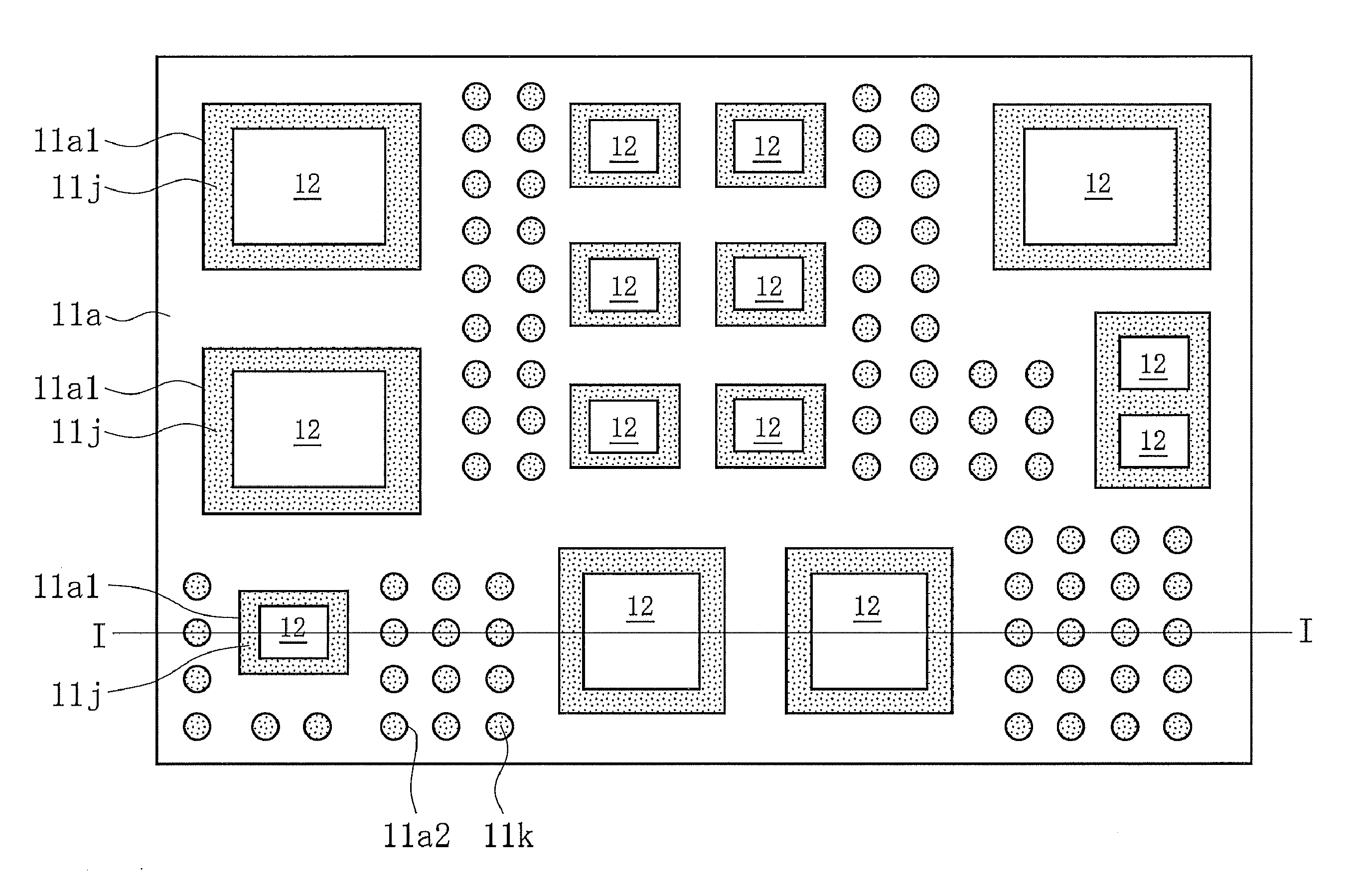
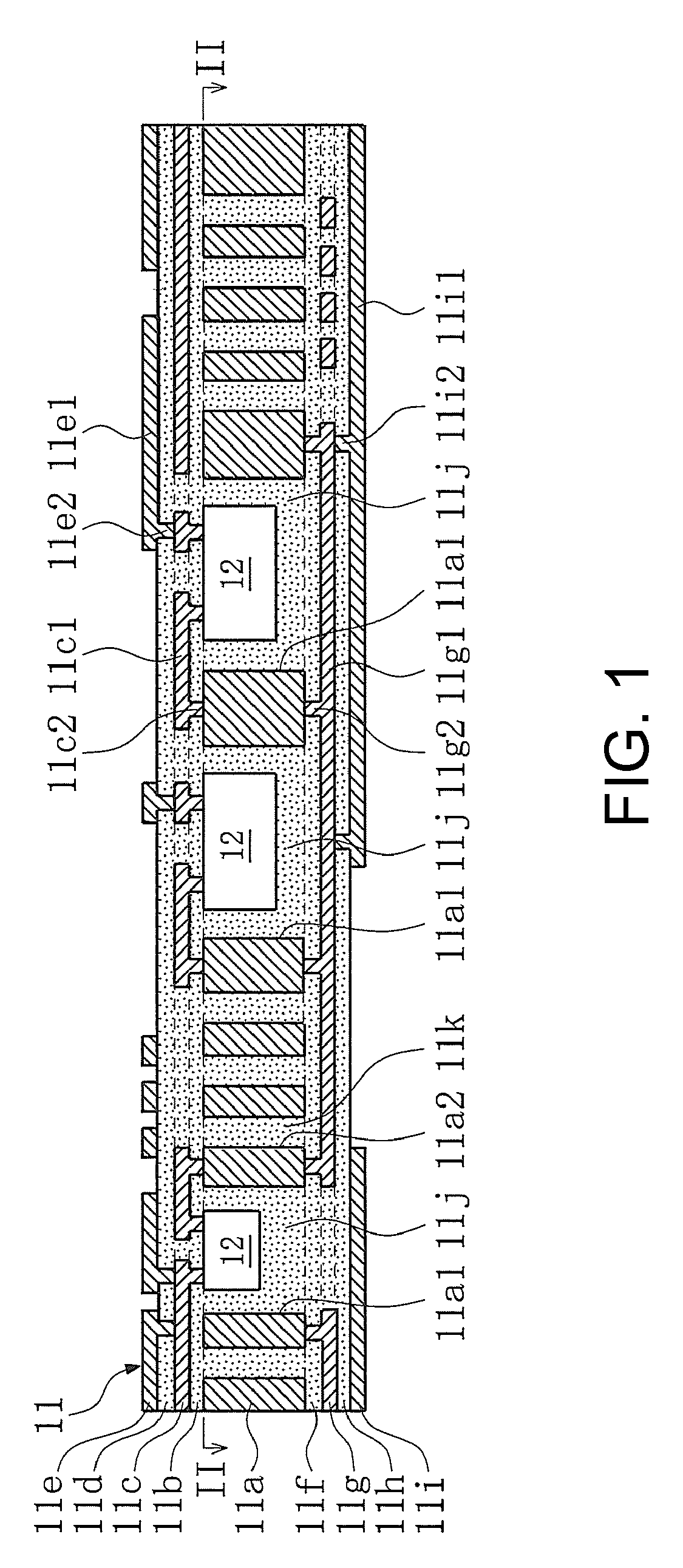
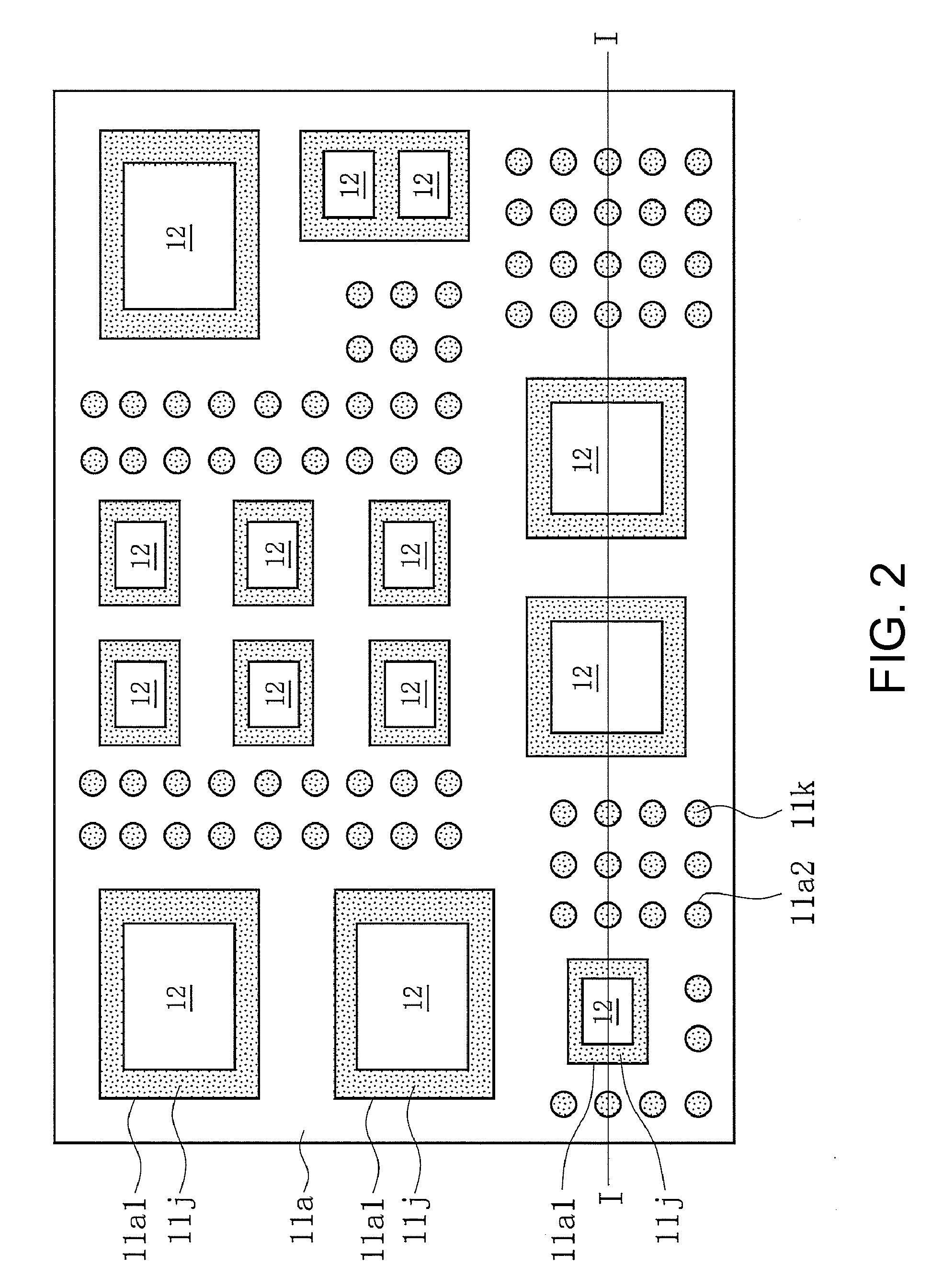
[0014]First, with reference to FIGS. 1 and 2, a configuration of the substrate with a built-in electronic component to which the present invention is applied will be explained. FIG. 1 is a cross-sectional view along the line I-I in FIG. 2, but the cross section of an electronic component 12 is not shown in FIG. 1.

[0015]The substrate with built-in electronic components (no reference character is given) shown in FIGS. 1 and 2 has a substrate 11 and a plurality of electronic components 12 built therein. In the substrate with built-in electronic components, a prescribed circuit that includes the plurality of electronic components 12 is constructed three-dimensionally through a core layer 11a described below, respective wiring lines 11c1, 11e1, 11g1, and 11i1 described below, and respective via conductors 11c2, 11e2, 11g2, and 11i2 described below.

[0016]The substrate 11 includes the core layer 11a having a prescribed thickness, a first insulating layer 11b formed on the top surface (firs...


PUM


Abstract

Provided is a substrate with a built-in electronic component that can minimize an occurrence of a deformation such as warping or distortion of the substrate with a built-in electronic component, which is caused by a difference in rigidity between a region of low rigidity and a region of high rigidity that are formed in a core layer thereof. In the substrate with a built-in electronic component, electronic components 12 are respectively housed in a plurality of housing portions 11a1 that are formed in a core layer 11a, and in the core layer 11a, a plurality of openings 11a2 filled with an insulator 11k are formed.

Description

[0001]This application claims the benefit of Japanese Application No. 2012-180211, filed in Japan on Aug. 15, 2012, which is hereby incorporated by reference in its entirety.TECHNICAL FIELD[0002]The present invention relates to a substrate with a built-in electronic component that has an electronic component built therein, and more particularly, to a substrate with a built-in electronic component in which an electronic component is housed in a housing portion that is formed in a core layer.BACKGROUND ART[0003]Patent Document 1 below discloses a substrate with a built-in electronic component that has a structure in which a core substrate made of an insulator has a plurality of penetrating holes penetrating the core substrate in the thickness direction, and electronic components are inserted in the respective penetrating holes. Electrodes (terminals) of each electronic component are connected to wiring lines on wiring boards that are disposed on the respective sides of the core substr...

Claims


Application Information

Patent Timeline
Patent Type & Authority Patents(United States)
IPC IPC(8): H05K1/16H05K1/18H05K3/46H05K1/02
CPCH05K1/16H05K1/185H05K3/4697H05K1/0271H05K2201/0187H01L24/19H01L2224/04105H01L2924/3511H05K3/46
Inventor SUGIYAMA, YUICHISAWATARI, TATSUROINOUE, YUSUKEMIYAZAKI, MASASHIHAMADA, YOSHIKIKAGAWA, TOSHIYUKI
Owner TAIYO YUDEN KK
Why Eureka
Try Eureka