
Single layer capacitive imaging sensors

a capacitive imaging and single-layer technology, applied in the field of single-layer capacitive imaging sensors, can solve the problems of the complexity the inability to meet the needs of the connection component, so as to reduce the overall physical size, reduce the system complexity, and reduce the effect of production cos

Active Publication Date: 2015-07-14
SYNAPTICS INC
View PDF231 Cites 74 Cited by
  • Summary
  • Abstract
  • Description
  • Claims
  • Application Information

AI Technical Summary

Benefits of technology

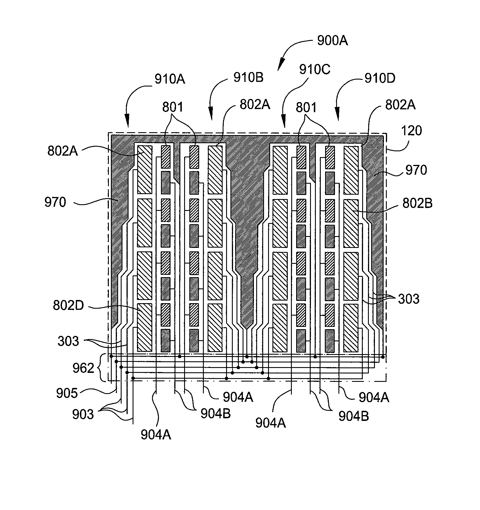
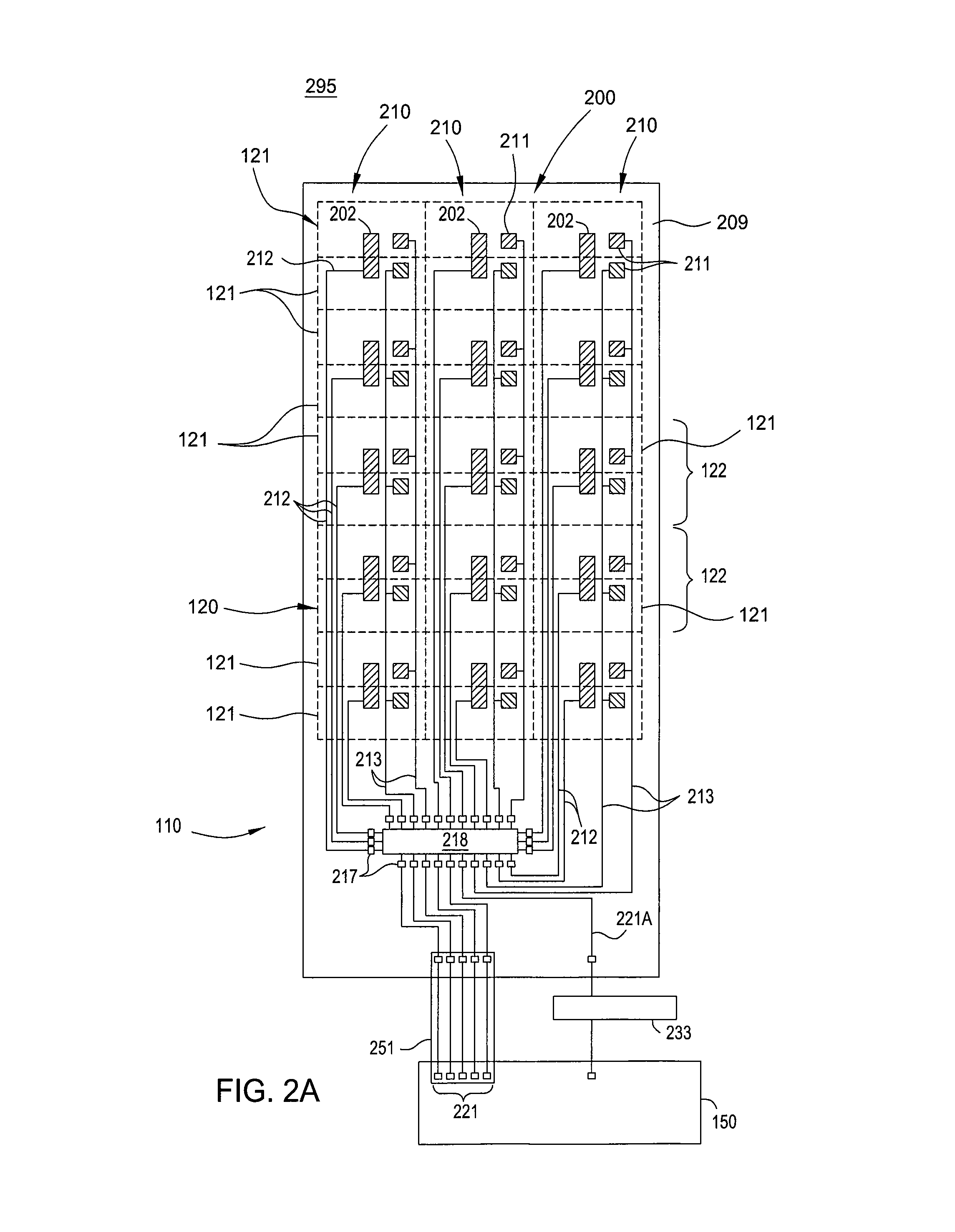
[0009]Embodiments of the invention generally provide an input device having a reduced system complexity, smaller overall physical size and low production cost. The input device described herein can provide more reliable and accurate position sensing data and / or position sensing results based on the signals generated by the interaction of an input object with an input region of the input device. Embodiments of the invention generally provide an input device that uses arrays of sensor electrodes and / or sensor electrode interconnection schemes to form the position sensing data. Embodiments of the invention described herein thus provide an improved apparatus and method for reliably sensing the presence of an object by a touch sensing device. Also, one or more of the embodiments described herein, utilizes one or more of the techniques and electrode array configurations disclosed herein to reduce or minimize the number of traces and / or sensor electrodes required to sense the position of an input object within the sensing region.

Problems solved by technology

Due to the often large number of sensor electrodes used to sense the presence and position of an input object with desirable accuracy, and also the need to connect each of these sensor electrodes to the various signal generation and data collection components in the electronic or computing system, the cost associated with forming these interconnections, the reliability of the system and the overall size of the of the proximity sensor device are often undesirably large and complex.
One will note that the cost and size limitations placed on the proximity sensor device are often created by the number of traces that are required, the number of required connection points, the connection component's complexity (e.g., number of pins on a connector) and the complexity of the flexible components used to interconnect the sensor electrodes to the control system.
Moreover, the greater the length of the traces used to interconnect the sensor electrodes to the computer system, the more susceptible the proximity sensor device is to interference, such as electromagnetic interference (EMI), commonly generated by the other supporting components.
The interference provided by these supporting components will adversely affect the reliability and accuracy of the data collected by the proximity sensing device.

Method used


Image

  • Single layer capacitive imaging sensors
  • Single layer capacitive imaging sensors
  • Single layer capacitive imaging sensors

Examples


Embodiment Construction

[0043]The following detailed description is merely exemplary in nature and is not intended to limit the invention or the application and uses of the invention. Furthermore, there is no intention to be bound by any expressed or implied theory presented in the preceding technical field, background, brief summary or the following detailed description.

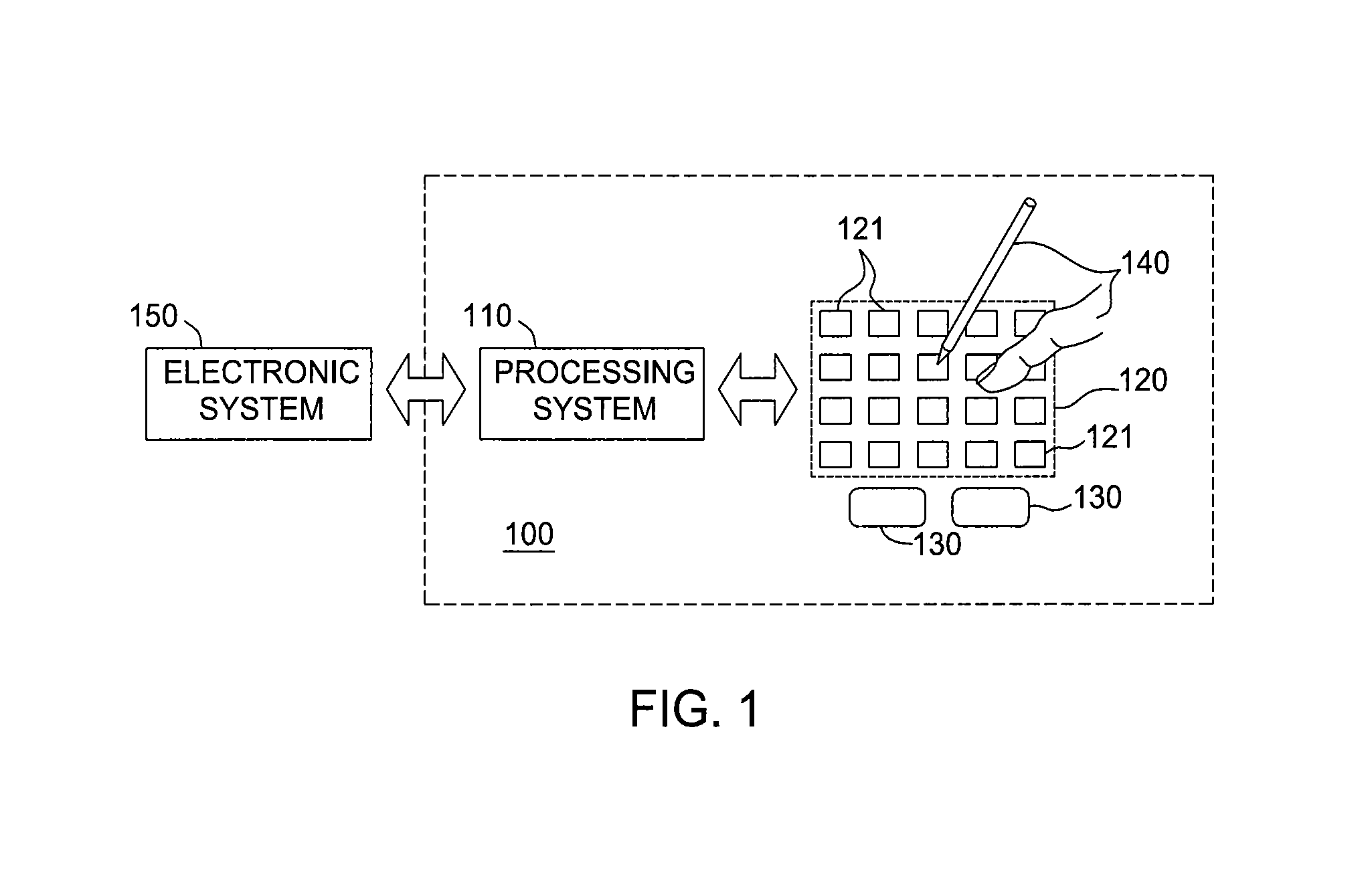
[0044]Embodiments of the invention generally provide an input device having a reduced system complexity, small overall physical size and low production cost. One or more of the embodiments discussed herein comprise an input device that includes a plurality of sensing elements that are interconnected in desired way to reliably and accurately acquire positional information of an input object. The acquired positional information may be used to control the system's operation mode, as well as graphical user interface (GUI) actions, such as cursor movement, selection, menu navigation, and other functions. In one embodiment, one or more capacitiv...


PUM


Abstract

Embodiments of the invention generally provide an input device that includes a plurality of sensing elements that are interconnected in desired way to acquire positional information of an input object, so that the acquired positional information can be used by other system components to control a display or other useful system components. One or more of the embodiments described herein, utilizes one or more of the techniques and sensor electrode array configuration disclosed herein to reduce or minimize the number of traces and / or electrodes required to sense the position of an input object within a sensing region of the input device.

Description

CROSS-REFERENCE TO RELATED APPLICATIONS[0001]This application claims benefit of U.S. provisional patent application Ser. No. 61 / 586,076, filed Jan. 12, 2012, which is herein incorporated by reference.BACKGROUND OF THE INVENTION[0002]1. Field of the Invention[0003]Embodiments of the present invention generally relate to a system and method for sensing an input object's position over a sensing region of a proximity sensing device.[0004]2. Description of the Related Art[0005]Input devices including proximity sensor devices, also commonly called touchpads or touch sensor devices, are widely used in a variety of electronic systems. A proximity sensor device typically includes a sensing region, often demarked by a surface, in which the proximity sensor device determines the presence, location and / or motion of one or more input objects. Proximity sensor devices may be used to provide interfaces for the electronic system. For example, proximity sensor devices are often used as input devices...

Claims


Application Information

Patent Timeline
Patent Type & Authority Patents(United States)
IPC IPC(8): G06F3/044
CPCG06F3/044G06F3/04164G06F3/0443G06F3/0448G06F3/041G06F2203/04112
Inventor BULEA, MIHAISOLVEN, DEREKREYNOLDS, JOSEPH KURTHHOCH, DAVIDDATTALO, TRACY SCOTT
Owner SYNAPTICS INC
Learn More