Touch sensing device and a method of fabricating the same using bonding marks on non-bonding surface of FPCB

a technology of touch sensing device and bonding mark, which is applied in the direction of fixed connections, inspection/indentification of circuits, instruments, etc., can solve the problems of reducing the reliability of the touch sensing device, the charge coupled device cannot perform contraposition between the touch panel and the flexible printing circuit board, etc., to reduce manpower demand, reduce production costs, and increase efficiency

Active Publication Date: 2015-08-18
TPK TOUCH SOLUTIONS (XIAMEN) INC
View PDF51 Cites 9 Cited by
  • Summary
  • Abstract
  • Description
  • Claims
  • Application Information

AI Technical Summary

Benefits of technology

[0008]The present disclosure improves mark position of a bonding mark of a touch sensing device, so as to make the bonding mark of the touch panel and the bonding mark of a flexible printing circuit board have a relationship of contraposition between them, and the contraposition can be simply performed by an optical sensing device or by naked eye, thereby enhancing precision of the contraposition to improve the reliability of the touch sensing device.
[0011]Therefore, in the fabricating, process of the present disclosure, the touch sensing device is designed for providing an optical sensing device for automatically positioning the touch panel and the flexible printing circuit board so as to increase efficiency and reduce the manpower demand for reducing the production cost, thereby increasing the precision of contraposition and enhancing the reliability of the bonding process to increase production yield of the touch sensing device.

Problems solved by technology

However, with a touch sensing device having a single-board touch panel as example, since a mask layer is directly disposed on the touch panel, the charge coupled device cannot perform contraposition between the touch panel and the flexible printing circuit board.
In view of this, if the contraposition and bond of the touch sensing device is performed at the position of the mask layer, the fabricating process of the touch sensing device reduces the reliability of the touch sensing device because of deficient precision.

Method used


Image

  • Touch sensing device and a method of fabricating the same using bonding marks on non-bonding surface of FPCB
  • Touch sensing device and a method of fabricating the same using bonding marks on non-bonding surface of FPCB
  • Touch sensing device and a method of fabricating the same using bonding marks on non-bonding surface of FPCB

Examples


Embodiment Construction

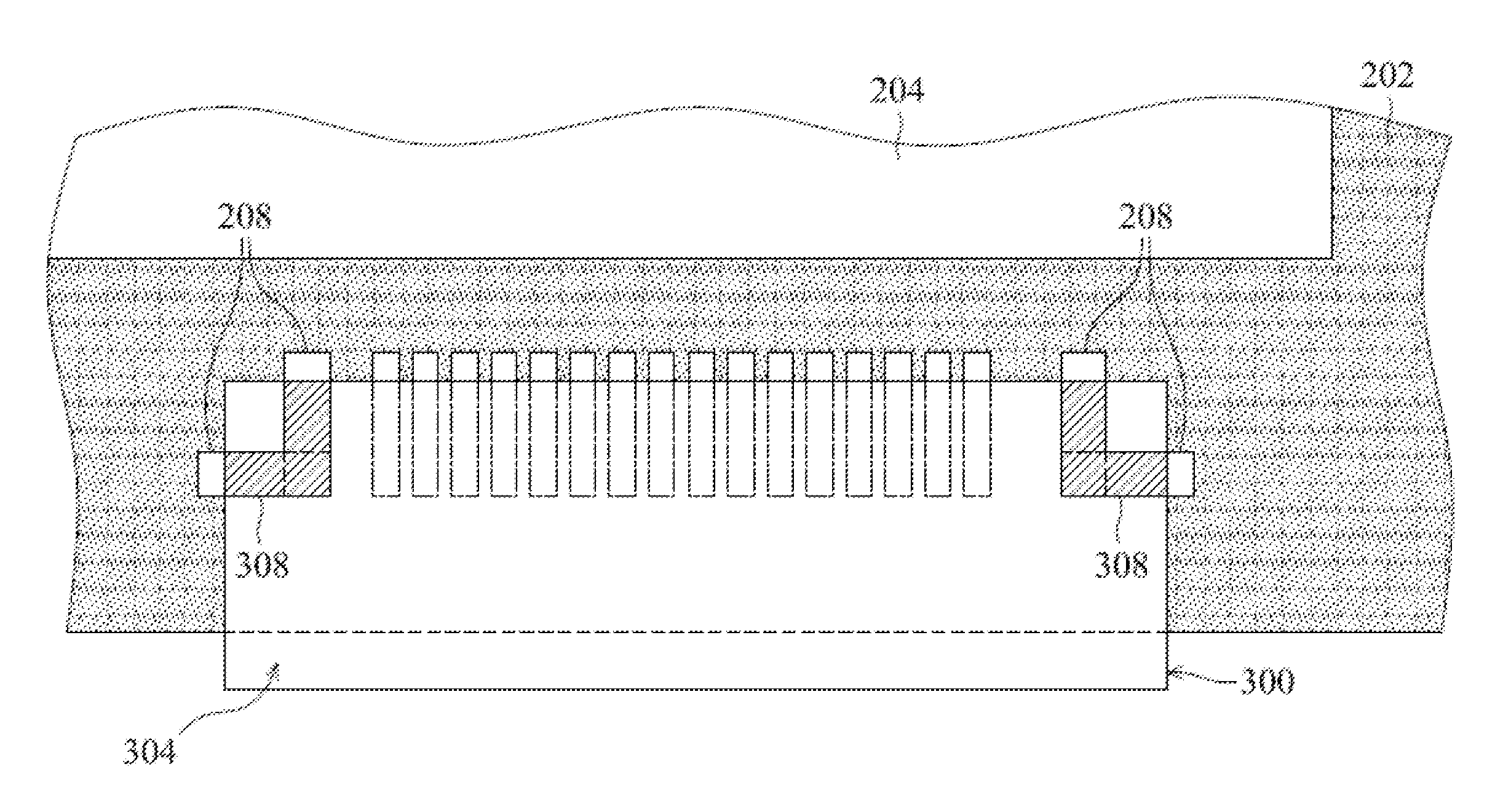
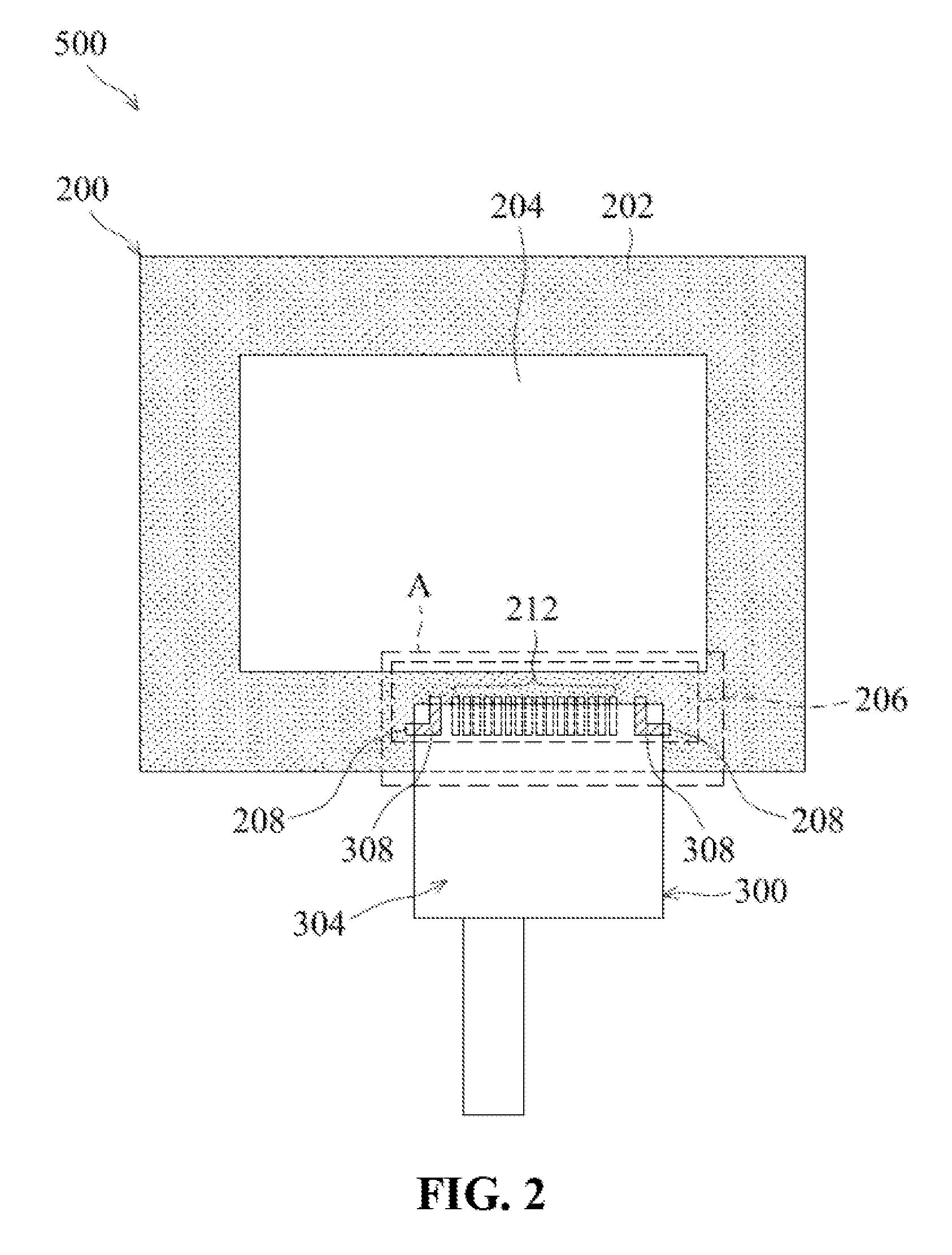
[0021]In the following descriptions accompanied with drawings of each embodiment, those similar or same parts all use same drawing numbers. In the drawings, shape or thickness of each embodiment can be amplified, and marked with simplified or convenient symbols. Furthermore, each component in the drawings is described separately, but those components that have not been shown or described are known to the person skilled in the art.

[0022]Touch sensing device of the present embodiment can include a single-board touch panel, a double-board touch panel, or a hybrid touch panel, wherein a mask layer can be disposed on the touch panel. The double-board touch panel comprises a protective substrate (cover lens) and a touch substrate and the single-board touch panel is designed to form a touch sensing electrode directly on the protective substrate, so as to omit a touch substrate as in the double-board touch panel. For convenient description, the following exemplary embodiments are illustrate...


PUM

PropertyMeasurementUnit
flexibleaaaaaaaaaa
lengthaaaaaaaaaa
L-shapeaaaaaaaaaa

Abstract

The present disclosure provides a touch sensing device and a method for fabricating the same. The touch sensing device comprises a touch panel and a flexible printed circuit board, wherein the touch panel comprises a first bonding mark and the flexible printed circuit board has a bonding surface bonded to the touch panel and has a non-bonding surface. The flexible printed circuit board comprises a second bonding mark disposed on the non-bonding surface. The second bonding mark and the first bonding mark have a relationship of contraposition.

Description

BACKGROUND OF THE INVENTION[0001]This Application claims the benefit of the People's Republic of China Application No. 201110401077.6, filed on November 27, 2011.FIELD OF THE INVENTION[0002]The present disclosure relates to a touch sensing device. More particularly, the present disclosure relates to a touch sensing device having a bonding mark for contraposition.DESCRIPTION OF THE RELATED ART[0003]In a known fabricating process of touch sensing devices, the process of bonding a touch panel with a flexible printing circuit generally utilizes a charge coupled device (CCD) to get a bonding mark disposed on the touch panel and flexible printing circuit board for positioning.[0004]However, with a touch sensing device having a single-board touch panel as example, since a mask layer is directly disposed on the touch panel, the charge coupled device cannot perform contraposition between the touch panel and the flexible printing circuit board. With reference to FIG. 1, FIG. 1 is a schematic ...

Claims


Application Information

Patent Timeline
Patent Type & Authority Patents(United States)
IPC IPC(8): H01H65/00H05K1/02H01L23/544H05K3/00H05K3/32H05K3/36H05K3/46G06F3/041G06F3/02H01R12/62
CPCH01H65/00G06F3/041H05K1/0269G06F3/0202G06F2203/04103H01L23/544H01R12/62H05K3/0008H05K3/323H05K3/361H05K3/4638H05K2201/09918H05K2201/10053H05K2201/10128H05K2203/166Y10T29/49105H01L2924/0002G06F3/04164H01L2924/00
Inventor CHEN, JIADONGHUANG, PINGPINGLUO, JIANXINGJIANG, YAU-CHEN
Owner TPK TOUCH SOLUTIONS (XIAMEN) INC
Why Eureka
Try Eureka