
Digital to analog converter and source driver chip thereof

a digital to analog converter and source driver technology, applied in the direction of instruments, static indicating devices, etc., can solve the problems of increasing the number of transistors in the transmission path, increasing the on-resistance of the transmission path, and increasing the transmission time accordingly

Active Publication Date: 2015-09-22
NOVATEK MICROELECTRONICS CORP
View PDF16 Cites 2 Cited by
  • Summary
  • Abstract
  • Description
  • Claims
  • Application Information

AI Technical Summary

Benefits of technology

[0013]It is therefore an objective of the present invention to provide a digital to analog converter and the source driver chip thereof capable of timely outputting Gamma voltages to a display to avoid abnormal display in many kinds of product applications.

Problems solved by technology

However, with the increase of definition, the quantity of transistors in the transmission paths may increase, such that on-resistance of the transmission paths may also increase, and the transmission time becomes longer accordingly.
Therefore, in many kinds of product applications with high image updating rate, data can not be transmitted timely, which may cause abnormal display.

Method used


Image

  • Digital to analog converter and source driver chip thereof
  • Digital to analog converter and source driver chip thereof
  • Digital to analog converter and source driver chip thereof

Examples


Embodiment Construction

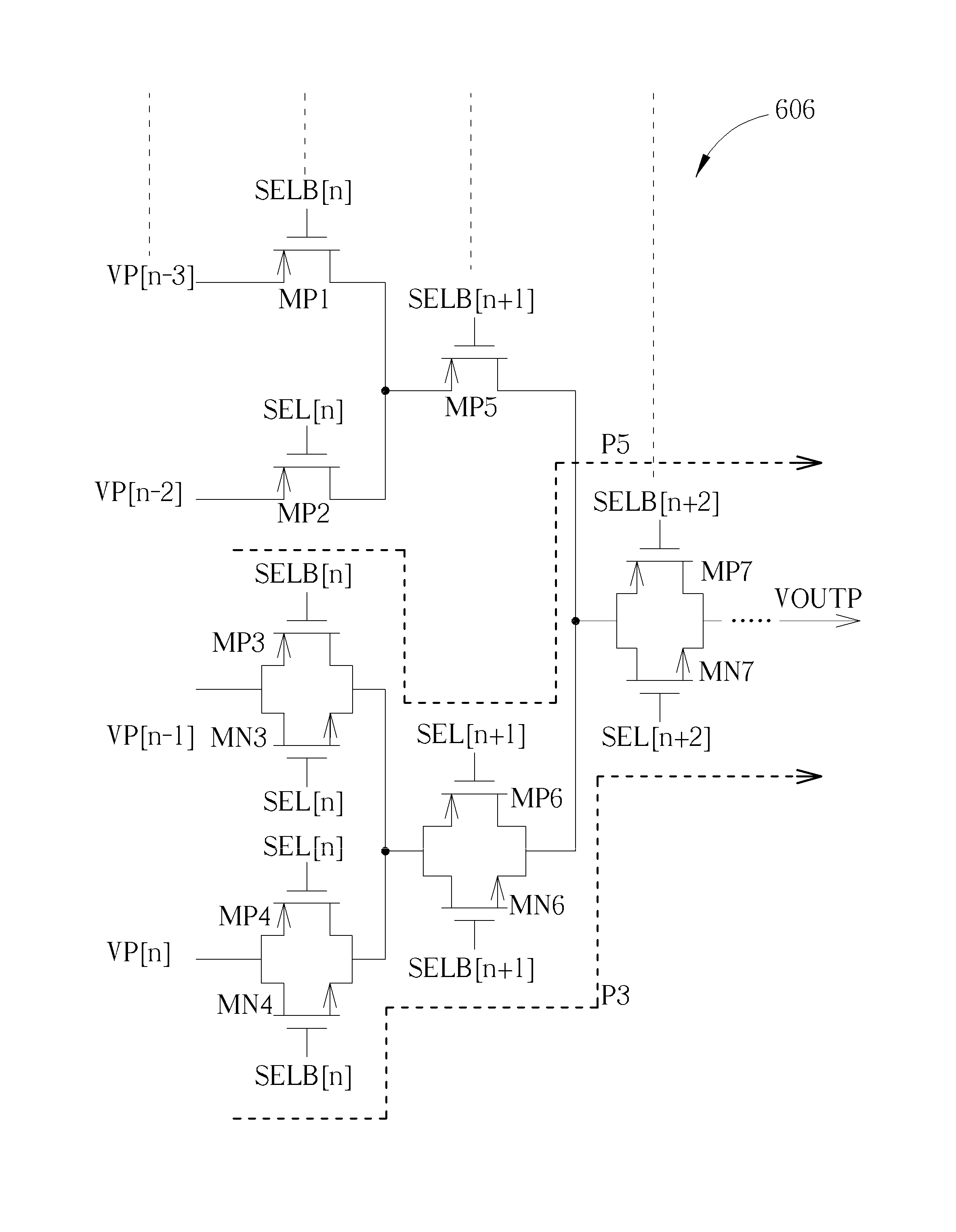
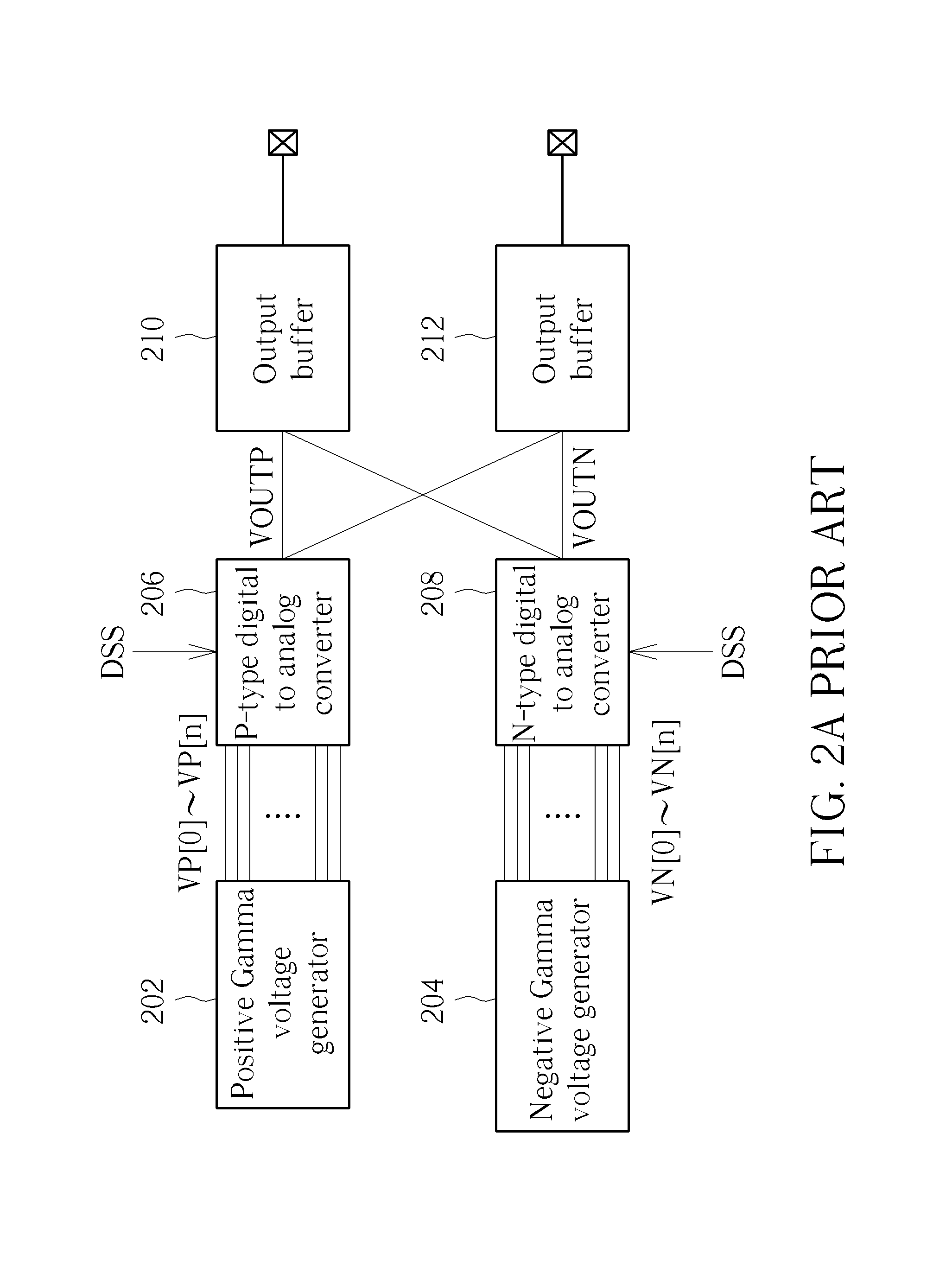
[0024]Please refer to FIG. 3A and FIG. 3B, which are schematic diagrams of partial circuits of a p-type digital to analog converter 306 and an n-type digital to analog converter 308 utilized for replacing the p-type digital to analog converter 206 and the n-type digital to analog converter 208 in FIG. 2A according to an embodiment of the present invention. The p-type digital to analog converter 306 is partially similar to the p-type digital to analog converter 206, and hence elements and signals with similar functions are denoted by the same symbols. The main difference between the p-type digital to analog converter 306 and the p-type digital to analog converter 206 is that a transmission path P2 corresponding to a receiving terminal receiving the positive Gamma voltage VP[n] closest to the middle voltage VDDA / 2 among the positive Gamma voltages VP[0]˜VP[n] (i.e. the minimal of the positive Gamma voltages VP[0]˜VP[n]) has lower on-resistance than transmission paths corresponding to ...


PUM


Abstract

A digital to analog converter for a source driver chip of a liquid crystal display device is disclosed. The digital to analog converter comprises an output terminal for outputting an output voltage, a plurality of receiving terminals for receiving a plurality of Gamma voltages, and a plurality of transmission paths comprising a plurality of first-type transistors coupled between the plurality of receiving terminals and the output terminal, respectively, for outputting one of the plurality of Gamma voltages as the output voltage according to a digital select signal; wherein a first transmission path corresponding to a first receiving terminal receiving a first Gamma voltage closest to a middle voltage among the plurality of Gamma voltages has lower on-resistance than other transmission paths among the plurality of transmission paths when a same source-to-gate voltage is applied.

Description

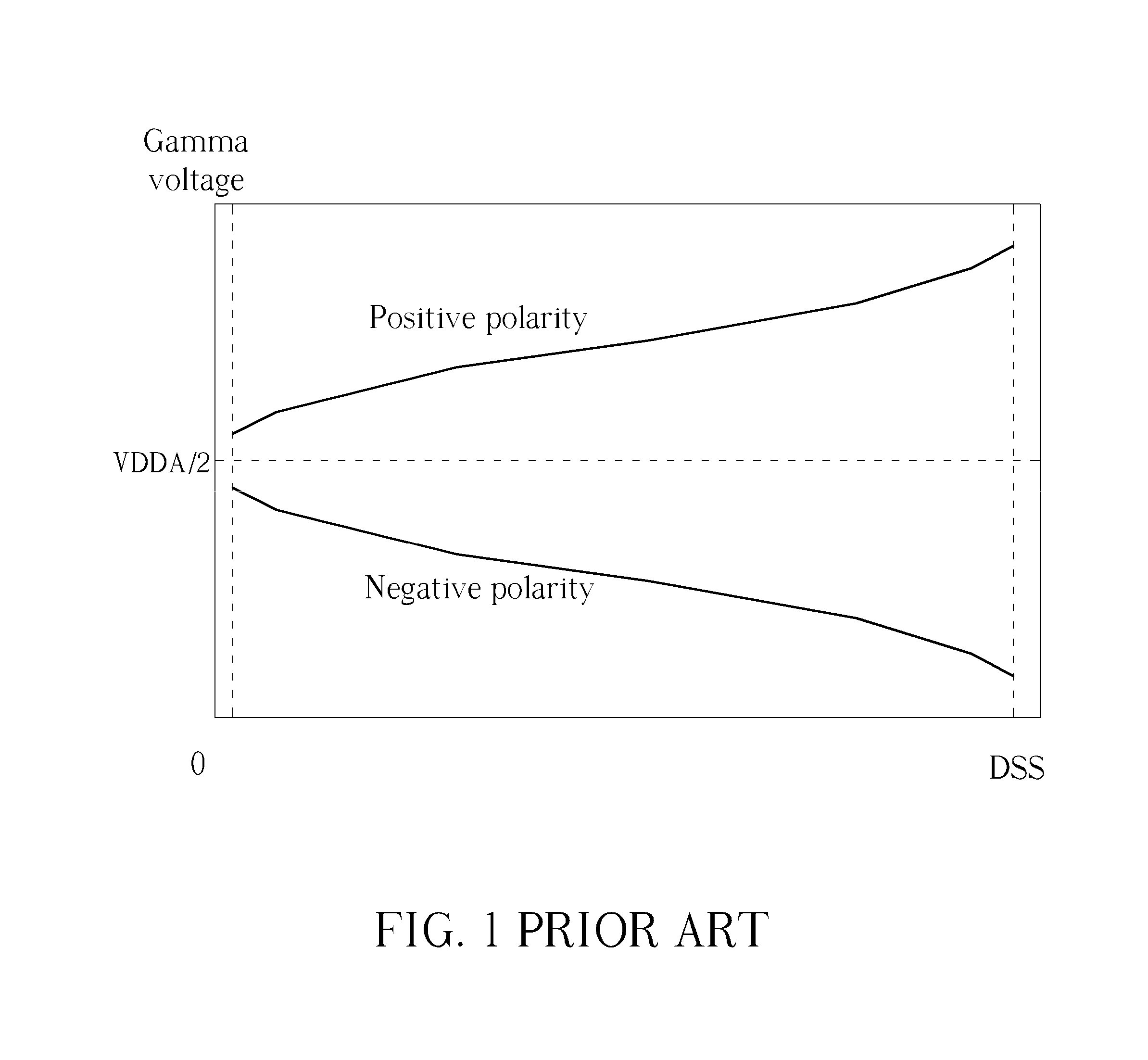
BACKGROUND OF THE INVENTION[0001]1. Field of the Invention[0002]The present invention relates to a digital to analog converter (DAC) and a source driver chip thereof, and more particularly, to a digital to analog converter and a source driver chip thereof capable of timely outputting Gamma voltages to a display to avoid abnormal display in many kinds of product applications.[0003]2. Description of the Prior Art[0004]In general, in a source driver chip of a liquid crystal display (LCD), a digital to analog converter may select a proper Gamma voltage from a plurality of Gamma voltages to output to an output stage according to a digital select signal, so as to drive a panel to display with accurate gray scales. In order to avoid continuously utilizing a voltage with a same polarity (e.g. positive polarity or negative polarity) to drive liquid crystal molecules, which reduces polarization or refraction of the liquid crystal molecules such that quality of image display deteriorates, the ...

Claims


Application Information

Patent Timeline
Patent Type & Authority Patents(United States)
IPC IPC(8): G09G3/36
CPCG09G3/36G09G3/3685G09G2310/027
Inventor CHENG, JHIH-SIOUHUANG, JU-LINHUNG, PANG-CHAN
Owner NOVATEK MICROELECTRONICS CORP
Learn More