Piezoelectric element with electrodes allowing substrate strain and method for manufacturing the same

a technology of electrodes and electrodes, applied in piezoelectric/electrostrictive device manufacturing/assembly, piezoelectric/electrostrictive device manufacturing/assembly, etc., can solve the problem of reducing the strain of ceramic substrates, and achieve the effect of less likely strain of piezoelectric elements

Active Publication Date: 2015-09-22
NGK INSULATORS LTD
View PDF16 Cites 2 Cited by
  • Summary
  • Abstract
  • Description
  • Claims
  • Application Information

AI Technical Summary

Benefits of technology

[0006]When the above-described piezoelectric effect or inverse piezoelectric effect is obtained, strain of the ceramic substrate is interrupted by rigidity of the electrodes formed on the respective surfaces of the ceramic substrate. This causes a problem in that an amount of strain of the ceramic substrate is reduced and the piezoelectric element becomes less likely to be strained. For example, when the piezoelectric effect is to be obtained in a case where the piezoelectric element is less likely to be strained, a voltage to be generated becomes small with respect to a force to be applied to the piezoelectric element. Furthermore, when the inverse piezoelectric effect is to be obtained in the case where the piezoelectric element is less likely to be strained, an amount of strain to be generated becomes small with respect to a voltage to be applied to the piezoelectric element. Accordingly, the present description provides a piezoelectric element having an electrode that is less likely to interrupt strain of a ceramic substrate.
[0008]In the piezoelectric element, the void is formed between the bottom of the groove and the electrode. That is, the electrode is not in contact with the ceramic substrate at the bottom of the groove. A part of the electrode which is not in contact with the ceramic substrate can be flexibly deformed as compared with a part of the electrode which is in contact with the ceramic substrate. Consequently, strain of the ceramic substrate is less likely to be interrupted by the electrode. Accordingly, the piezoelectric element is readily strained.

Problems solved by technology

This causes a problem in that an amount of strain of the ceramic substrate is reduced and the piezoelectric element becomes less likely to be strained.

Method used


Image

  • Piezoelectric element with electrodes allowing substrate strain and method for manufacturing the same
  • Piezoelectric element with electrodes allowing substrate strain and method for manufacturing the same
  • Piezoelectric element with electrodes allowing substrate strain and method for manufacturing the same

Examples


embodiment

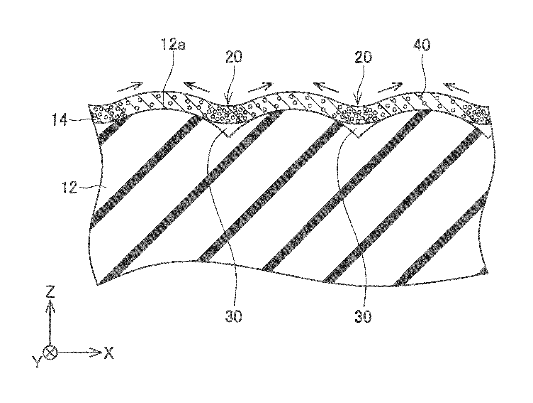
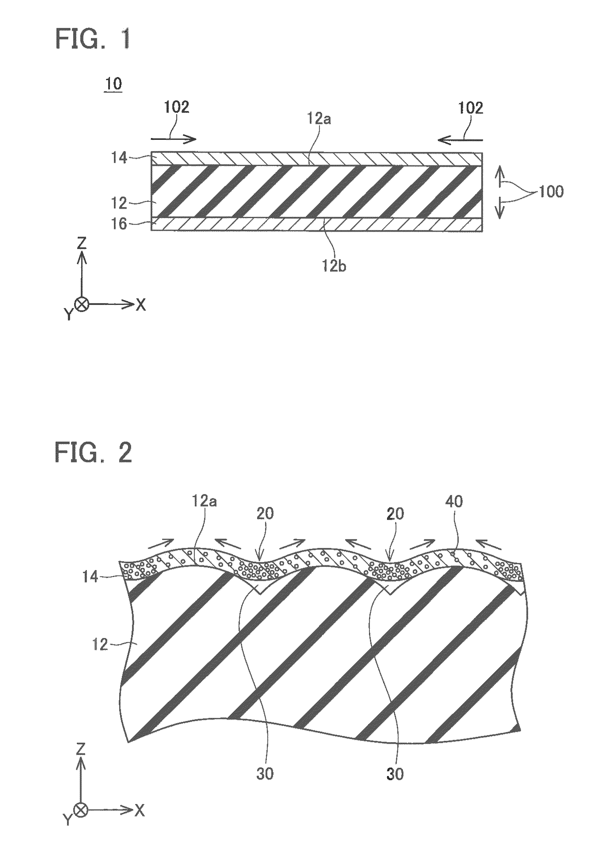
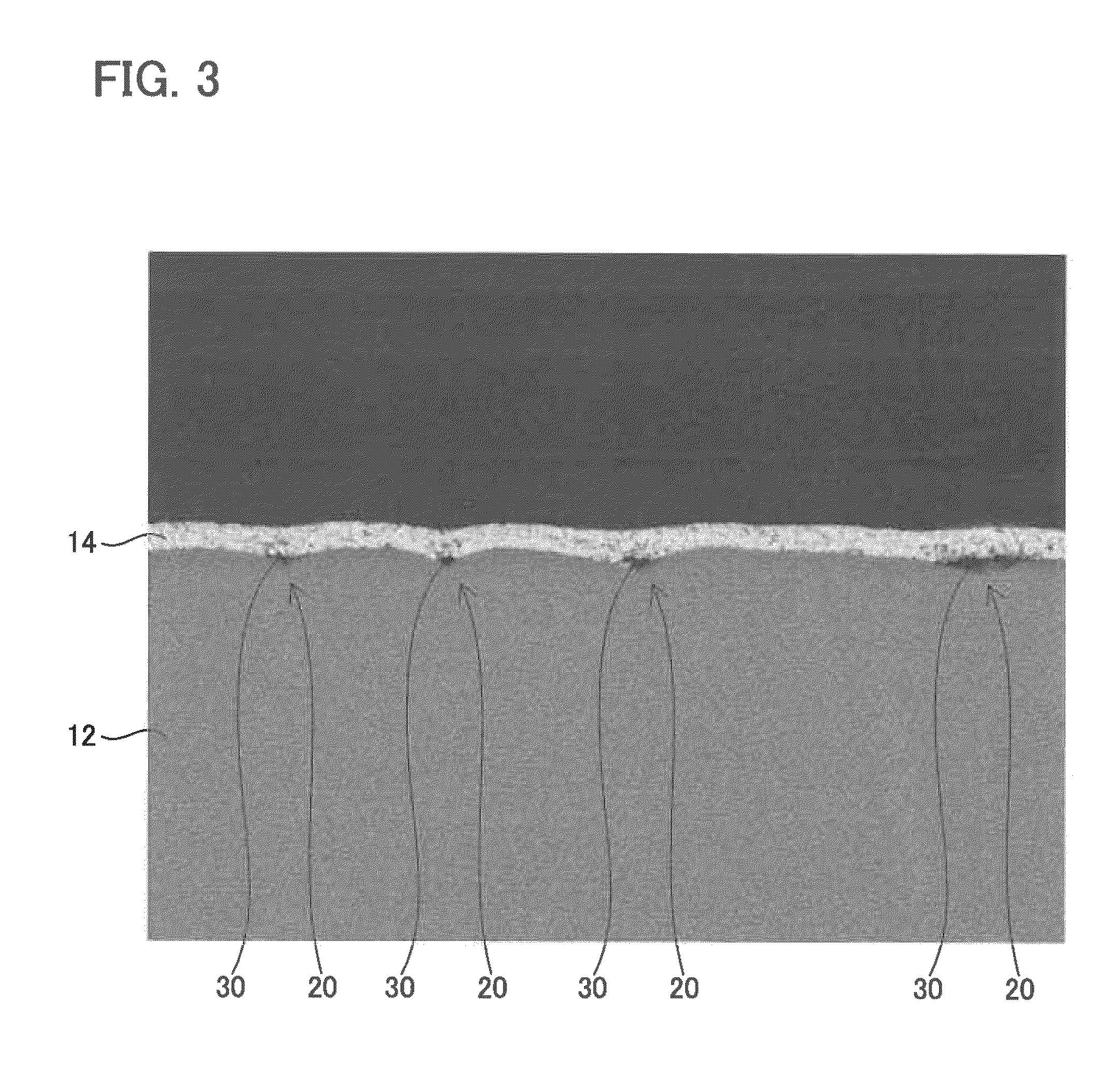
[0037]As illustrated in FIG. 1, a piezoelectric element 10 of an embodiment includes a ceramic substrate 12, an electrode 14, and an electrode 16. The electrode 14 is formed on an upper surface 12a of the ceramic substrate 12. The electrode 16 is formed on a lower surface 12b of the ceramic substrate 12. The ceramic substrate 12 is constituted by a piezoelectric body. Note that, hereinafter, a thickness direction of the ceramic substrate 12 may be referred to as a Z direction, a direction perpendicular to the Z direction (a direction along the upper surface of the ceramic substrate 12) may be referred to as an X direction, and a direction perpendicular to both of the X direction and the Z direction may be referred to as a Y direction. Note that, the piezoelectric element 10 is subjected to a polarization treatment by an electric field oriented toward the electrode 16 from the electrode 14.

[0038]When a voltage is applied between the electrode 14 and the electrode 16 such that the ele...


PUM

PropertyMeasurementUnit
thicknessaaaaaaaaaa
thicknessaaaaaaaaaa
sizeaaaaaaaaaa

Abstract

A piezoelectric element is provided with a ceramic substrate including a first surface on which a groove is formed, and a first electrode formed on the first surface of the ceramic substrate and including a crossing part that extends over the groove. At least one void is formed between a bottom of the groove and the crossing part of the first electrode.

Description

CROSS-REFERENCE TO RELATED APPLICATION[0001]This application claims priority to Japanese Patent Application No. 2012-034937 filed on Feb. 21, 2012, the contents of which are hereby incorporated by reference into the present application.BACKGROUND OF THE INVENTION[0002]1. Field of the Invention[0003]The present application relates to a piezoelectric element.[0004]2. Description of Related Art[0005]A piezoelectric element includes a ceramic substrate and electrodes formed on respective surfaces of the ceramic substrate. When an external force is applied to the ceramic substrate of the piezoelectric element, the ceramic substrate is strained and a voltage is generated between the electrodes (piezoelectric effect). Furthermore, when a voltage is applied between the electrodes of the piezoelectric element, an electric field is applied to the ceramic substrate to strain the ceramic substrate (inverse piezoelectric effect). Note that a piezoelectric element having a plurality of internal e...

Claims


Application Information

Patent Timeline
Patent Type & Authority Patents(United States)
IPC IPC(8): H01L41/047H01L41/29
CPCH01L41/047H01L41/29Y10T29/42H10N30/87H10N30/06
Inventor OHNISHI, TAKAOSHIMIZU, HIDEKIUETANI, MASAYUKI
Owner NGK INSULATORS LTD
Why Eureka
Try Eureka