Display device and electronic device

a technology of electronic devices and display devices, applied in the field of display devices, can solve problems such as viewer strain, achieve the effects of reducing viewer strain, reducing viewer strain, and great depth

Active Publication Date: 2013-11-14
SEMICON ENERGY LAB CO LTD
View PDF8 Cites 16 Cited by
  • Summary
  • Abstract
  • Description
  • Claims
  • Application Information

AI Technical Summary

Benefits of technology

[0012]The present invention is made in view of the foregoing technical background. Therefore, an object of one embodiment of the present invention is to provide a display device that can display an image which causes a viewer less strain associated with viewing and gives a viewer a great sense of depth. Further, an object of one embodiment of the present invention is to provide an electronic device for enjoying an image which causes a viewer less strain associated with viewing and gives a viewer a great sense of depth.
[0038]According to one embodiment of the present invention, it is possible to provide a display device that can display an image which causes a viewer less strain associated with viewing and gives a viewer a great sense of depth. Further, it is possible to provide an electronic device for enjoying an image which causes a viewer less strain associated with viewing and gives a viewer a great sense of great depth.

Problems solved by technology

Thus, there has been a problem in that the difference has caused strain on the viewer.

Method used


Image

  • Display device and electronic device
  • Display device and electronic device
  • Display device and electronic device

Examples


embodiment 1

[0053]In this embodiment, a structural example of a display device according to one embodiment of the present invention is described with reference to drawings.

Structural Example

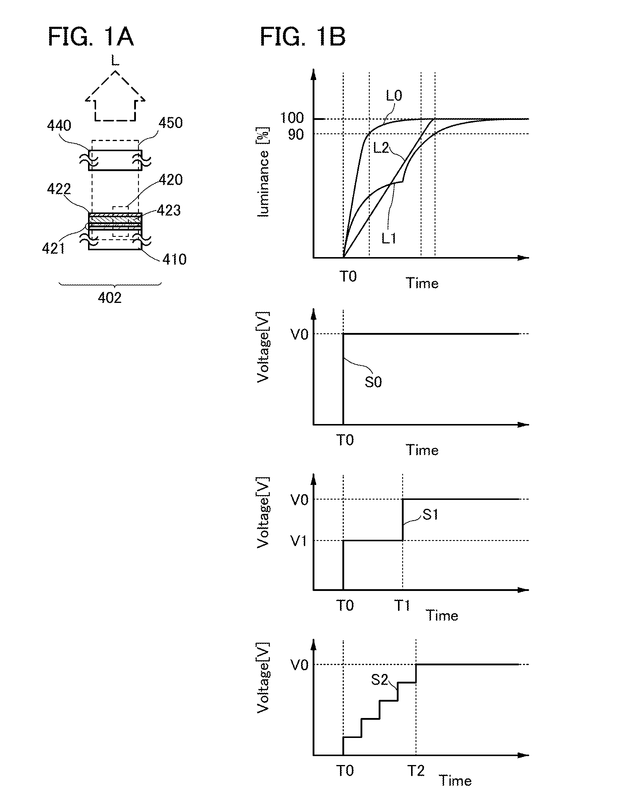
[0054]FIG. 1A schematically shows a structural example of a light-emitting module that can be used for a pixel portion of a display device according to one embodiment of the present invention.

[0055]In a pixel 402, a light-emitting module 450 is provided. The light-emitting module 450 includes a first substrate 410, a second substrate 440, and a light-emitting element 420 sealed between the first substrate 410 and the second substrate 440 which are bonded to each other with an unshown sealant. The light-emitting element 420 includes a first electrode 421 formed over the first substrate 410, a second electrode 422 overlapping with the first electrode 421, and a layer 423 containing a light-emitting organic compound between the first electrode 421 and the second electrode 422.

[0056]The first electrode 421 shown...

embodiment 2

[0135]In this embodiment, a structural example of a display device according to one embodiment of the present invention and a structural example of a display panel which can be used for the display device according to one embodiment of the present invention will be described.

[Structure of Display Panel]

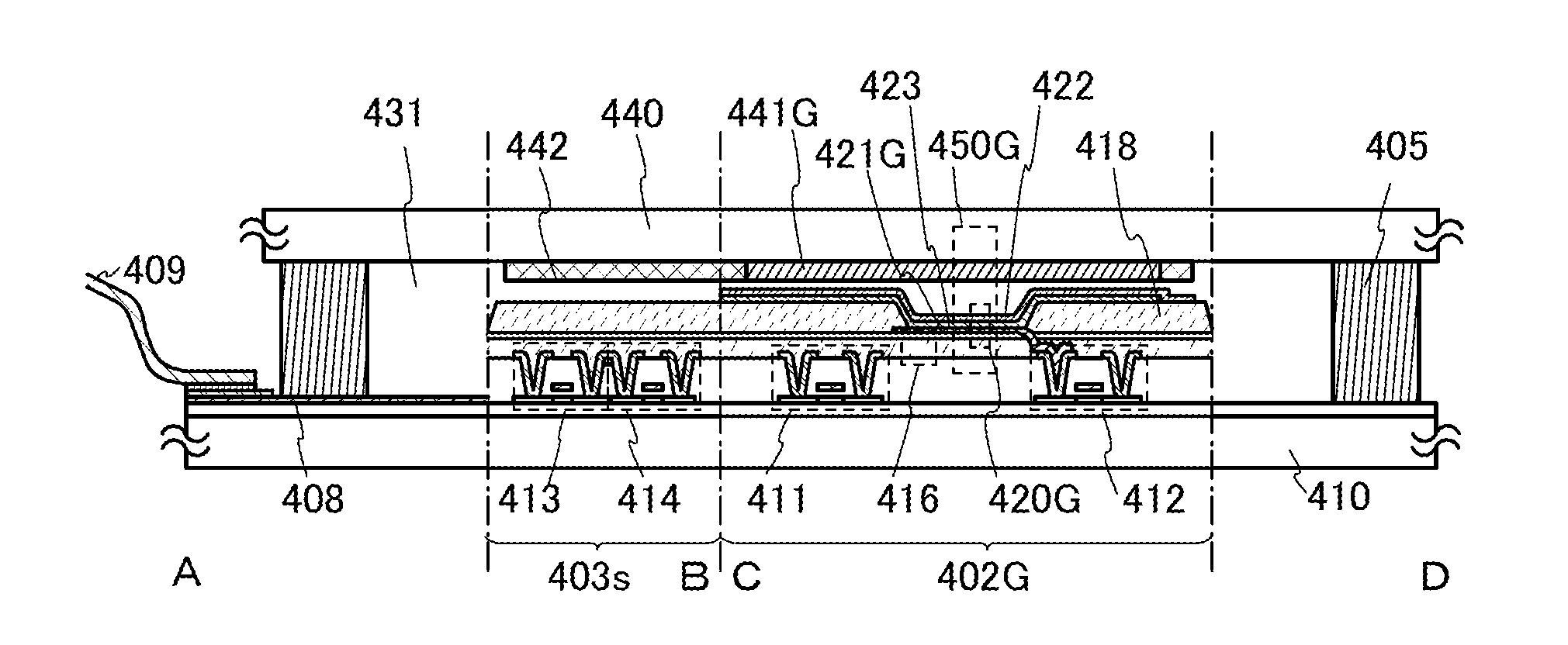
[0136]FIGS. 7A to 7C show a structure of a display panel which can be used for the display device according to one embodiment of the present invention. FIG. 7A is a top view of a structure of a display panel which can be used for the display device according to one embodiment of the present invention, FIG. 7B is a side view of a structure including a cross section taken along line A-B and C-D in FIG. 7A, and FIG. 7C is a side view of a structure of a pixel including a cross section taken along line E-F in FIG. 7A.

[0137]A display panel 400 shown as an example in this embodiment includes a display portion 401 over a first substrate 410. The display portion 401 includes a plurality of pi...

modification example

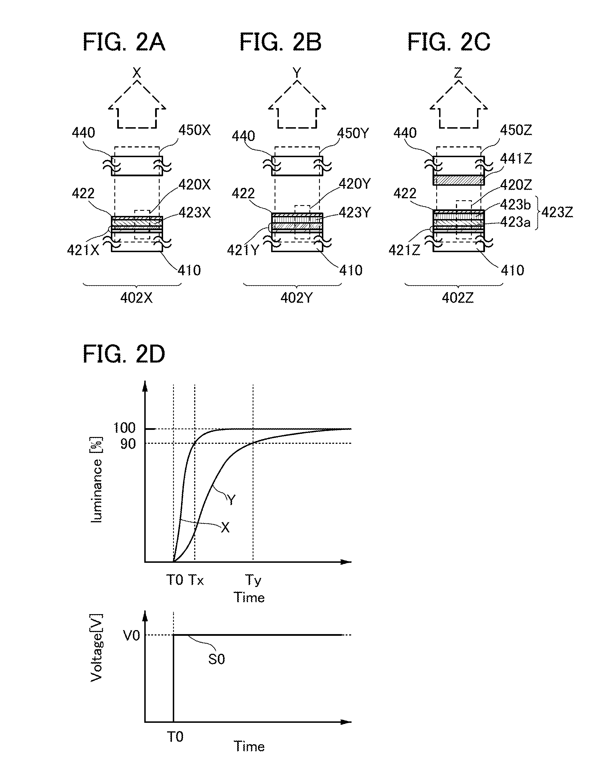
[0187]FIGS. 8A and 8B show a modification example of this embodiment. FIG. 8A is a side view of a structure including cross sections taken along line A-B and C-D in FIG. 7A, and FIG. 8B is a side view of a structure of a pixel including a cross section taken along line E-F in FIG. 7A.

[0188]A display panel shown in FIGS. 8A and 8B is a modification example of the display panel shown in FIGS. 7A to 7C and has a pixel structure different from that in the display panel shown in FIGS. 7A to 7C. Specifically, the display panel shown in FIGS. 8A and 8B is different from the display panel shown in FIGS. 7A to 7C in that the color filter is not provided and in that sub-pixels of different emission colors include layers containing different light-emitting organic compounds. A modification example of a structure of the pixel 402 included in the display portion 401 is described with reference to FIG. 8B.

[0189]The pixel 402 shown as the modification example in this embodiment includes the sub-pi...


PUM


Abstract

A display device has an NTSC ratio of higher than or equal to 80% and a contrast ratio of higher than or equal to 500 and includes a display portion. In the display portion, a pixel is provided at a resolution of greater than or equal to 80 ppi, and the pixel includes a light-emitting module capable of emitting light with a spectral line half-width of less than or equal to 60 nm. Further, the light emission of the light-emitting module is raised to a desired luminance with a gradient of greater than or equal to 0 in response to an input signal within a response time of longer than or equal to 1 μs and shorter than 1 ms.

Description

BACKGROUND OF THE INVENTION[0001]1. Field of the Invention[0002]The present invention relates to a display device. Further, the present invention relates to an electronic device including a display device.[0003]2. Description of the Related Art[0004]A display device that displays a stereoscopic image using a binocular parallax is known. Such a display device is configured to display, on one screen, an image to be seen from the position of the left eye of a viewer (an image for left eye) and an image to be seen from the position of the right eye of the viewer (an image for right eye). The viewer sees the image for left eye with the left eye and the image for right eye with the right eye and is thus allowed to see a stereoscopic image.[0005]For example, in a glasses system, an image for left eye and an image for right eye are alternately displayed on a screen of a display device in synchronization with a shutter provided in a pair of glasses, whereby the left eye of a viewer is allowe...

Claims


Application Information

Patent Timeline
Patent Type & Authority Applications(United States)
IPC IPC(8): G02B27/22G02B30/00
CPCG02B27/22G09G3/003G09G3/3233G09G3/3291H04N13/144H04N13/302G02B30/00H10K59/30H10K59/38H10K50/852G09G3/20H10K50/125H10K50/13H10K50/856H10K2102/301G02B30/27
Inventor YAMAZAKI, SHUNPEIHIRAKATA, YOSHIHARU
Owner SEMICON ENERGY LAB CO LTD
Why Eureka
Try Eureka