

Iii-nitride light emitting device
- Summary
- Abstract
- Description
- Claims
- Application Information
AI Technical Summary
Benefits of technology
Problems solved by technology
Method used
Image

Examples
example 1
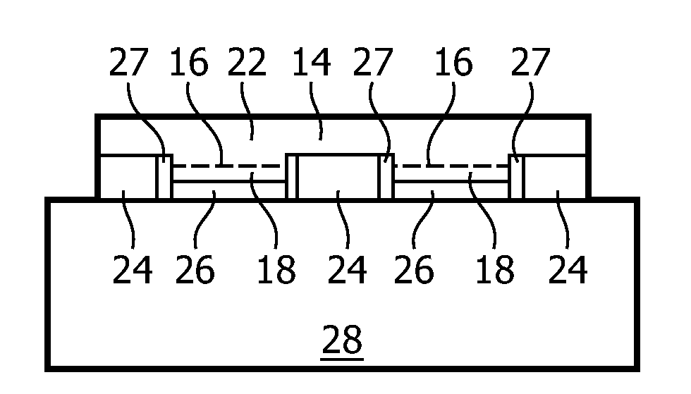
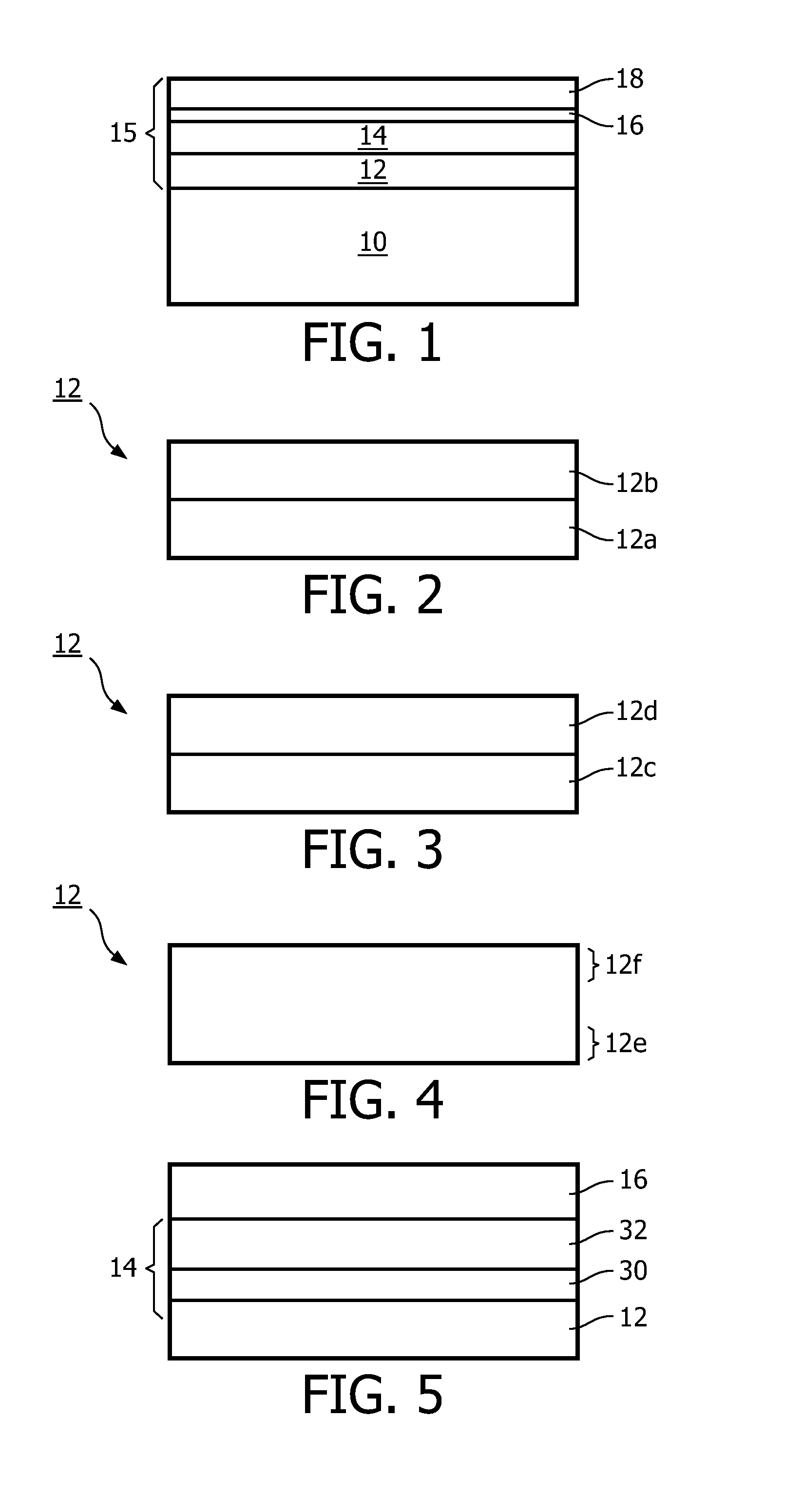
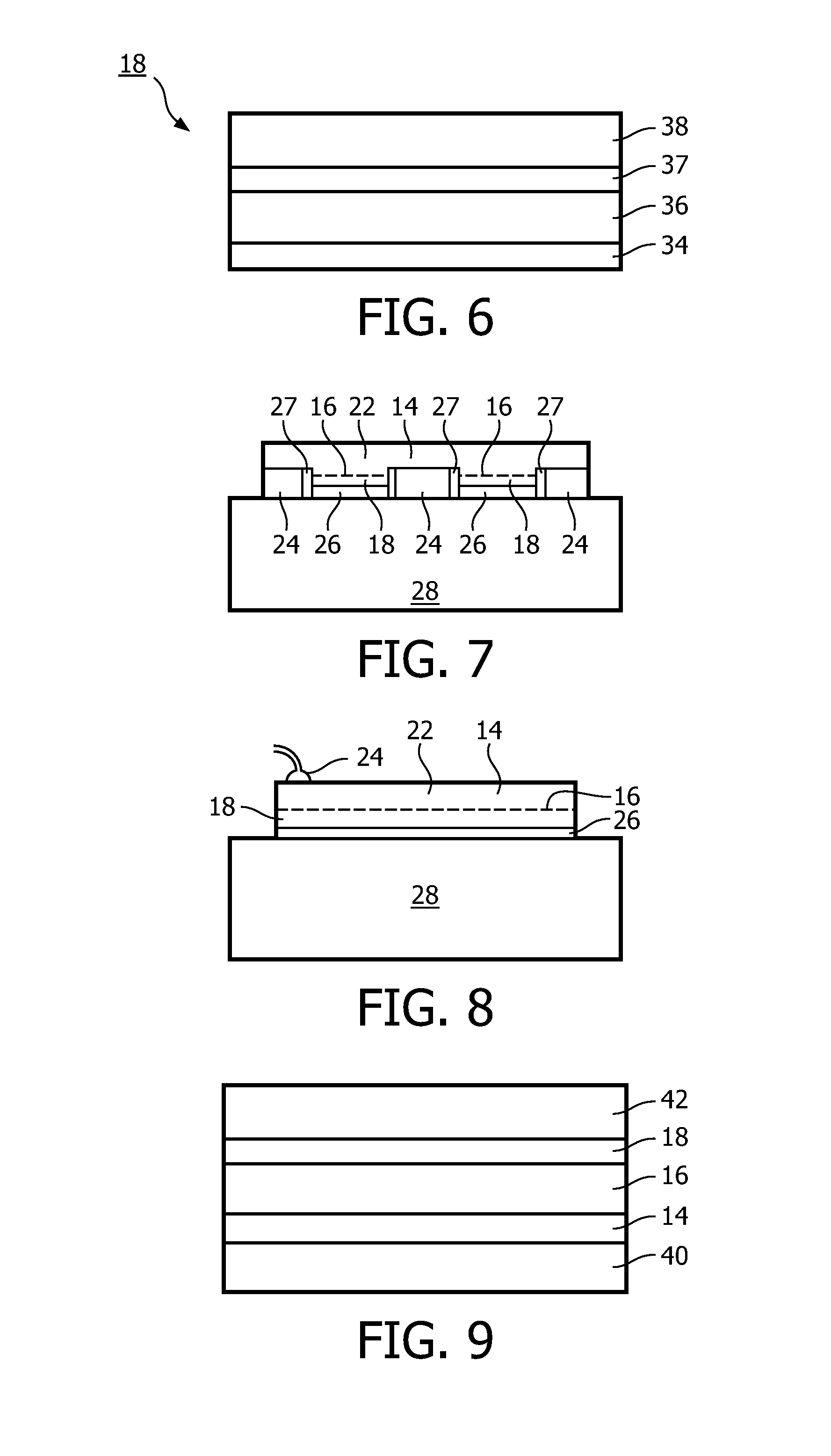
[0073]An Al-free LED grown on a ScAlMgO4 substrate includes a 1-6 μm thick In0.14 Ga0.86N base layer 12 doped with 1×10¹⁸ to 1×1019cm−3 Si, followed by an active region 16 including In0.15-0.20Ga0.85-0.8N quantum wells of 2-5 nm thickness separated by barriers composed of In0.10-0.16Ga0.9-0.84N with 1-6 nm thickness, all nominally un-doped. Active region 16 is followed by a 2-10 nm thick In0.10-0.16Ga0.9-0.84N cap layer 34, a 10-40 nm thick In0.0-0.13Ga1-0.87N electron blocking layer 36 doped with Mg to 1×1020 cm−3, and a 60-120 nm thick In0.14 Ga0.86N p-contact layer 38 doped with Mg at a concentration of 1×10¹⁸ to 1×1019cm−3 for the first 85 nm, then ramped to 5×10¹⁹ to 2×1020cm−3 for the final 1-10 nm.
example 2
[0074]An Al-free LED including a pit-filling layer is grown on a ScAlMgO4 substrate. A 1-6 μm thick In0.14 Ga0.86N base layer 12 is doped with 1×10¹⁸ to 1×1019cm−3 Si, followed by a 1-20 nm thick pit-filling layer composed of In0.0-0.13Ga1-0.87N doped similarly to the base layer. The active region 16 includes In0.15-0.20Ga0.85-0.8N quantum wells of 2-5 nm thickness separated by barriers composed of In0.10-0.16Ga0.9-0.84N with 1-6 nm thickness, all nominally un-doped. Active region 16 is followed by a 2-10 nm thick In0.10-0.16Ga0.9-0.84N cap layer 34, 10-40 nm In0.0-0.13Ga1-0.87N electron blocking layer 36 doped with Mg to 1×1020cm−3, and 60-120 nm thick In0.14 Ga0.86N p-contact layer 38 doped with Mg at a concentration of 1×10¹⁸ to 1×1019cm−3 for the first 85 nm, then ramped to 5×10¹⁹ to 2×1020cm−3 for the final 1-10 nm.
example 3
[0075]An Al-free LED grown on a ScAlMgO4 substrate includes a 1-6 μm thick In0.14 Ga0.86N base layer 12 doped with 1×10¹⁸ to 1×1019cm−3 Si, followed by a spacer composed of In0.10-0.16Ga0.9-0.84N doped 2e18 to 2e19 cm−3 with Si. The active region 16 includes In0.15-0.20Ga0.85-0.8N quantum wells of 2-5 nm thickness separated by barriers composed of In0.10-0.16Ga0.9-0.84N with 1-6 nm thickness, all nominally un-doped. This stack is followed by a 2-10 nm thick In0.10-0.16Ga0.9-0.84N cap layer 34, 10-40 nm In0.0-0.13Ga1-0.87N electron blocking layer 36 doped with Mg to 1×1020cm−3, and 60-120 nm thick In0.14 Ga0.86N p-contact layer 38 doped with Mg at a concentration of 1×10¹⁸ to 1×1019cm−3 for the first 85 nm, then ramped to 5×10¹⁹ to 2×1020cm−3 for the final 1-10 nm.
PUM
 Abstract
Description
Claims
Application Information