Microwave heating apparatus and processing method

a technology of microwave heating and processing methods, applied in microwave heating, electrical apparatus, electric/magnetic/electromagnetic heating, etc., can solve the problems of deterioration of electrical characteristics of devices, difficulty in miniaturizing design, and excessive depth of diffusion layer, so as to improve heating efficiency and power use efficiency.

Active Publication Date: 2015-12-01
TOKYO ELECTRON LTD
View PDF12 Cites 2 Cited by
  • Summary
  • Abstract
  • Description
  • Claims
  • Application Information

AI Technical Summary

Benefits of technology

[0009]In view of the above, the present invention provides a microwave heating apparatus and a processing method which are capable of uniformly processing a target object while improving power use efficiency and heating efficiency.
[0019]In the microwave heating apparatus and the processing method in accordance with the aspects of the present invention, the loss of the microwaves radiated into the processing chamber is reduced, so that the power use efficiency and the heating efficiency can be improved. Further, the target object can be uniformly heated.

Problems solved by technology

However, in the RTA process, as the diffusion of the doping atoms progresses, the depth of the diffusion layer exceeds a tolerable range, and this makes the miniaturized design difficult.
Since the depth of the diffusion layer is incompletely controlled, the electrical characteristics of devices deteriorate.
For example, a problem such as occurrence of leakage current or the like is generated.
When a plurality of microwave introduction ports is provided, microwaves introduced from one of the microwave introduction ports may enter another microwave introduction port, thereby deteriorating power usage efficiency and heating efficiency

Method used


Image

  • Microwave heating apparatus and processing method
  • Microwave heating apparatus and processing method
  • Microwave heating apparatus and processing method

Examples


first embodiment

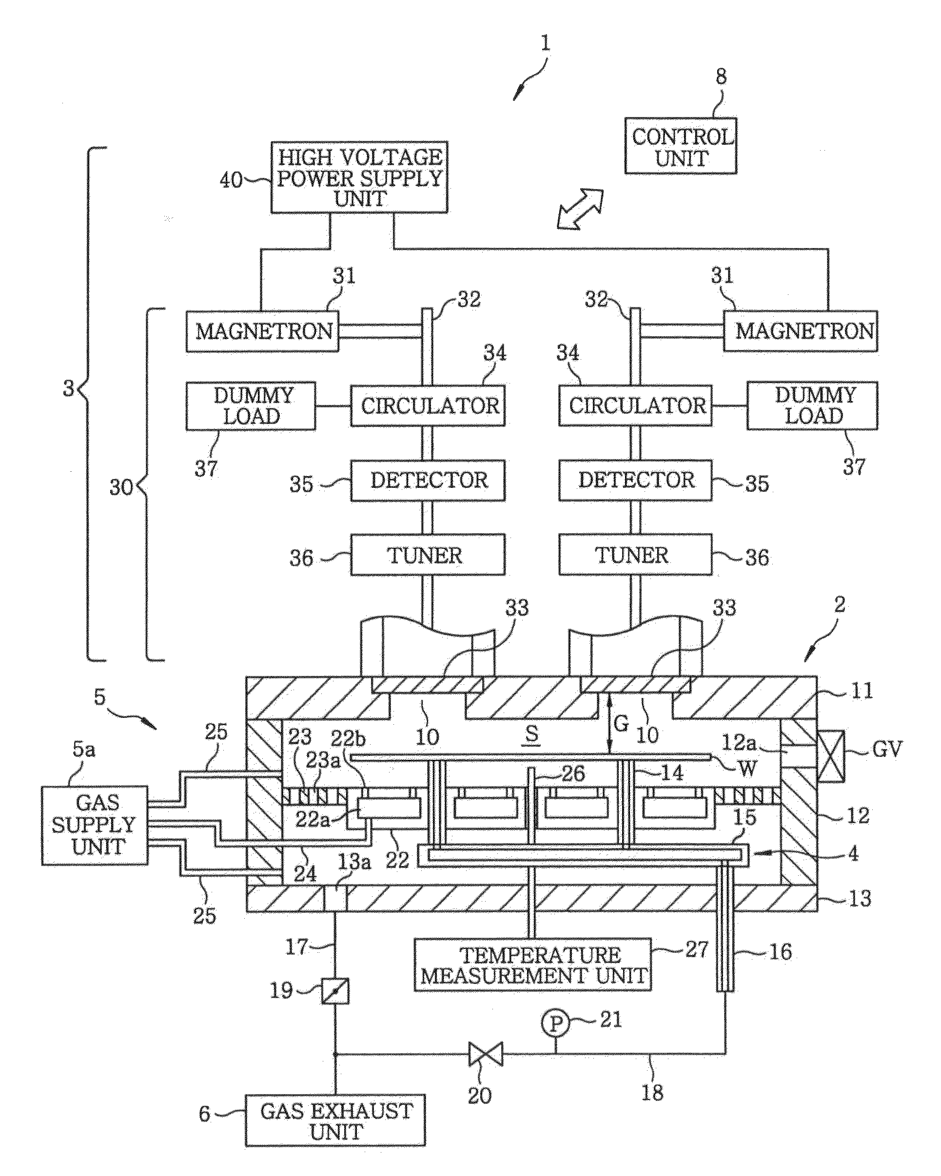
[0041]First, a schematic configuration of a microwave heating apparatus in accordance with a first embodiment of the present invention will be described with reference to FIG. 1. FIG. 1 is a cross sectional view showing a schematic configuration of the microwave heating apparatus in accordance with the present embodiment. The microwave heating apparatus 1 of the present embodiment performs an annealing process by irradiating microwaves to, e.g., a semiconductor wafer (hereinafter, simply referred to as “wafer”) for manufacturing semiconductor devices through a series of consecutive operations.

[0042]The microwave heating apparatus 1 includes: a processing chamber 2 accommodating a wafer W as a target object to be processed; a microwave introducing unit 3 for introducing microwaves into the processing chamber 2; a supporting unit 4 for supporting a wafer W in the processing chamber 2; a gas supply mechanism 5 for supplying a gas into the processing chamber 2; a gas exhaust unit 6 for ...

second embodiment

[0145]Next, a microwave heating apparatus in accordance with a second embodiment of the present invention will be described with reference to FIGS. 10 and 11. FIG. 10 is a cross sectional view showing a schematic configuration of a microwave heating apparatus 1A of the present embodiment. FIG. 11 explains a rectifying plate 23A of the microwave heating apparatus 1A of the present embodiment which serves as a microwave reflection mechanism.

[0146]The microwave heating apparatus 1A of the present embodiment includes a processing chamber 2 for accommodating a wafer W as a target object to be processed; a microwave introducing unit 3 for introducing microwaves into the processing chamber 2; a supporting unit 4 for supporting the wafer W in the processing chamber 2; a gas supply mechanism 5A for supplying a gas into the processing chamber 2; a gas exhaust unit 6 for vacuum-evacuating the processing chamber 2; and a control unit 8 for controlling the respective components of the microwave ...

third embodiment

[0156]Hereinafter, a microwave heating apparatus in accordance with a third embodiment of the present invention will be described with reference to FIGS. 12 to 14. FIG. 12 is a cross sectional view showing a schematic configuration of a microwave heating apparatus 1B of the present embodiment. FIG. 13 explains a state in which a microwave introducing adaptor 50 serving as an adaptor member having a waveguide for transmitting microwaves is installed at the ceiling portion 11. FIG. 14 explains grooves formed at the microwave introducing adaptor 50.

[0157]The microwave heating apparatus 1B of the present embodiment performs annealing by radiating microwaves to the wafer W for manufacturing semiconductor devices through a plurality of consecutive operations. In the following description, the difference between the microwave heating apparatus 1B of the present embodiment and the microwave heating apparatus 1 of the first embodiment will be described. In the microwave heating apparatus 1B ...


PUM


Abstract

In the microwave heating apparatus, four microwave introduction ports are arranged at positions spaced apart from each other at an angle of about 90° in a ceiling portion of a processing chamber in such a way that the long sides and the short sides thereof are in parallel to inner surfaces of four sidewalls. The microwave introduction port are disposed in such a way that each of the microwave introduction ports are not overlapped with another microwave introduction port whose long sides are in parallel to the long sides of the corresponding microwave introduction port when the corresponding microwave introduction port is moved in translation in a direction perpendicular to the long sides thereof.

Description

CROSS-REFERENCE TO RELATED APPLICATIONS[0001]This application claims priority to Japanese Patent Application Nos. 2011-289024 and 2012-179802 filed on Dec. 28, 2011 and Aug. 14, 2012, respectively, the entire contents of which are incorporated herein by reference.FIELD OF THE INVENTION[0002]The present invention relates to a microwave heating apparatus for performing a predetermined process by introducing microwaves into a processing chamber and a processing method for heating a target object to be processed by using the microwave heating apparatus.BACKGROUND OF THE INVENTION[0003]As an LSI device or a memory device is miniaturized, a depth of a diffusion layer in a transistor manufacturing process is decreased. Conventionally, doping atoms implanted into the diffusion layer are activated by a high-speed heating process referred to as an RTA (Rapid Thermal Annealing) using a lamp heater. However, in the RTA process, as the diffusion of the doping atoms progresses, the depth of the d...

Claims


Application Information

Patent Timeline
Patent Type & Authority Patents(United States)
IPC IPC(8): H05B6/64H05B6/72H05B6/74H05B6/80H05B6/70
CPCH05B6/6402H05B6/70H05B6/806H05B6/72H05B6/6426H05B6/707H01L21/268
Inventor IKEDA, TAROKASAI, SHIGERUYAMASHITA, JUNBAN, MASAKAZU
Owner TOKYO ELECTRON LTD
Why Eureka
Try Eureka