Electronic grade glass substrate and making method

a technology of electronic grade glass and substrate, applied in the direction of manufacturing tools, lapping machines, instruments, etc., can solve the problems of cracking of the corner between the side and bottom surfaces of the recess, and the cracking of the corner. , to achieve the effect of high strength and cleanness, increased strength of the bottom wall, and high accuracy

Active Publication Date: 2015-12-08
SHIN ETSU CHEM IND CO LTD
View PDF20 Cites 2 Cited by
  • Summary
  • Abstract
  • Description
  • Claims
  • Application Information

AI Technical Summary

Benefits of technology

[0023]The invention is useful in the manufacture of an electronic grade synthetic quartz glass substrate having a recess, channel or step, for example, a synthetic quartz glass substrate for use as a photomask substrate in the photolithography or a mold substrate in the nanoimprint lithography (NIL) for the fabrication of IC and other electronic devices. In the electronic grade glass substrate having a recess, channel or step, the bottom and side surfaces of the recess, channel or step are mirror finished, and shape factors are consistently controlled at a high accuracy. Thus the substrate is unsusceptible to fissure and chipping at the recess, channel or step and has a high strength and cleanness.
[0024]Since the corner between the side and bottom surfaces of the recess, channel or step where the maximum stress is exerted when a load is applied to the recess, channel or step is curvilinear chamfered, the strength of the bottom wall is increased. Even when a certain load is applied to the recess, channel or step to introduce a change in its shape, the bottom wall is robust enough to prevent breakage.

Problems solved by technology

This is problematic in that the recess, channel or step is susceptible to fissure and chipping at its edges or corners, and the corners are difficult to polish to mirror finish.
When the substrate is mounted in a lithography or NIL apparatus, the substrate comes in physical contact with the apparatus, which can raise problems because the recess, channel or step is susceptible to fissure and chipping at its edges or corners.
The prior art configuration has the problem that because of difficulty of the machining and polishing steps, the corner between the side and bottom surfaces of the recess, channel or step has a potential of cracking, and it is difficult to maintain the strength at the bottom of the recess, channel or step in a consistent manner.
This gives rise to the problem that the substrate can be relatively readily broken when repetitive loads are applied thereto.

Method used


Image

  • Electronic grade glass substrate and making method
  • Electronic grade glass substrate and making method
  • Electronic grade glass substrate and making method

Examples


example 1

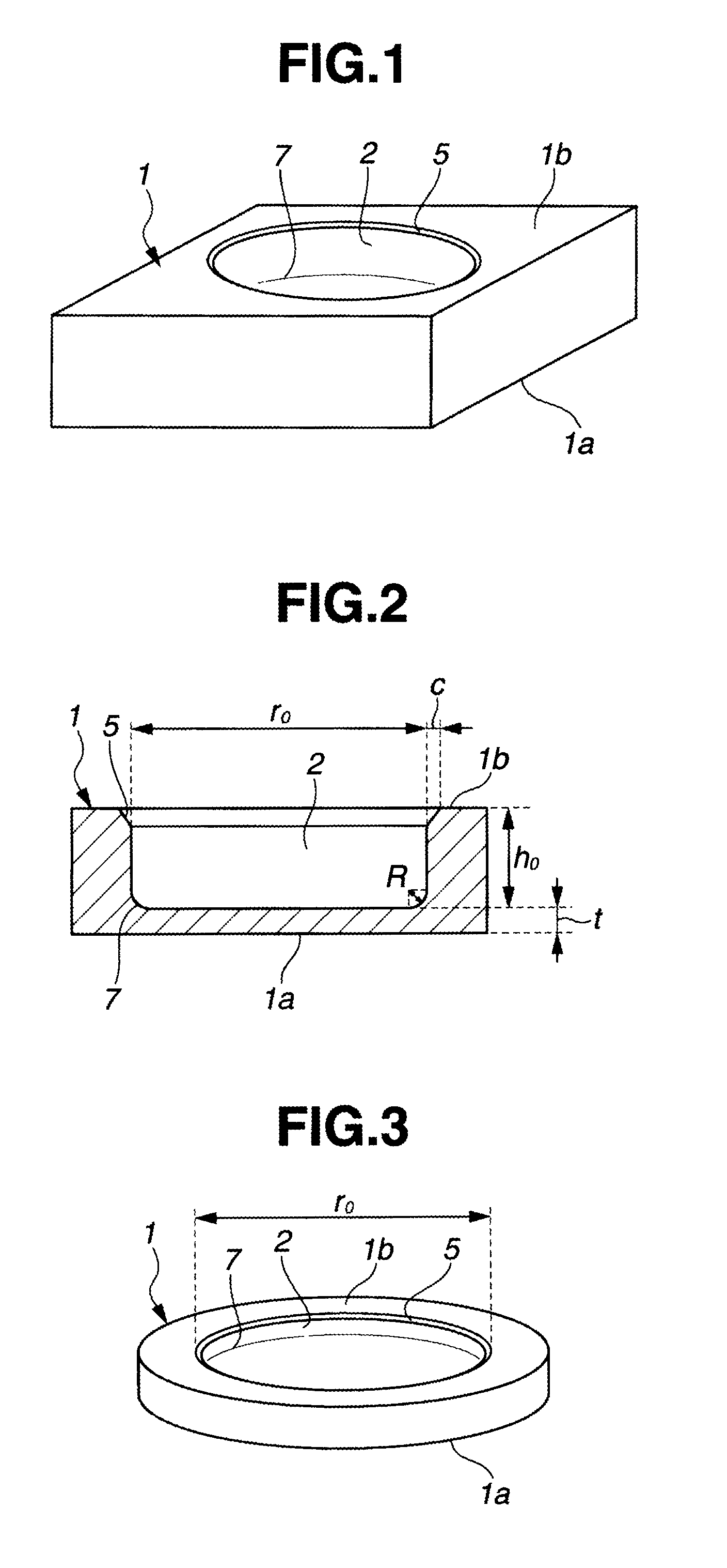
[0072]A synthetic quartz glass substrate A dimensioned 100 mm×100 mm×6.35 mm (thick) having front, back and end surfaces polished to mirror finish was prepared as a starting substrate. Using a machining center and a diamond abrasive wheel, the starting substrate was machined at the center of its back surface to form a circular recess with a depth of 5.32 mm and a diameter of 69.98 mm, having a first chamfer with a width of 0.3 mm between the recess side surface and the substrate back surface.

[0073]Next, the machined substrate was fixedly mounted on a platform. A wool felt buff having a diameter of 50 mm and a height of 30 mm adapted to rotate at 1,000 rpm was forced in contact with the bottom surface of the recess under 3,500 Pa and the side surface under 2,000 Pa. The substrate-holding platform was rotated at 10 rpm, whereby the surfaces were polished for 60 minutes to mirror finish. The recess (or counterbore) in the glass substrate as polished had a depth of 5.35 mm with a bottom...

example 2

[0083]A synthetic quartz glass substrate A dimensioned 100 mm×100 mm×6.35 mm (thick) having front, back and end surfaces polished to mirror finish was prepared as a starting substrate. Using a machining center and a diamond abrasive wheel, the starting substrate was machined at the center of its back surface to form a circular recess with a depth of 5.32 mm and a diameter of 69.98 mm, having a curvilinear second chamfer with a radius of curvature of 1.5 mm between the recess side and bottom surfaces and a first chamfer with a width of 0.3 mm between the recess side surface and the substrate back surface.

[0084]Next, the machined substrate was fixedly mounted on a platform. A wool felt buff having a diameter of 50 mm and a height of 30 mm adapted to rotate at 1,000 rpm was forced in contact with the bottom surface of the recess under 3,500 Pa and the side surface under 2,000 Pa. The substrate-holding platform was rotated at 10 rpm, whereby the surfaces were polished for 60 minutes to ...

example 3

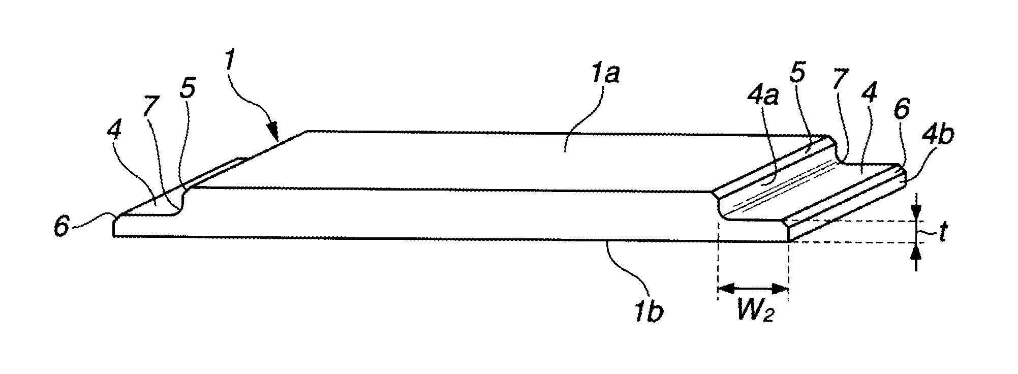
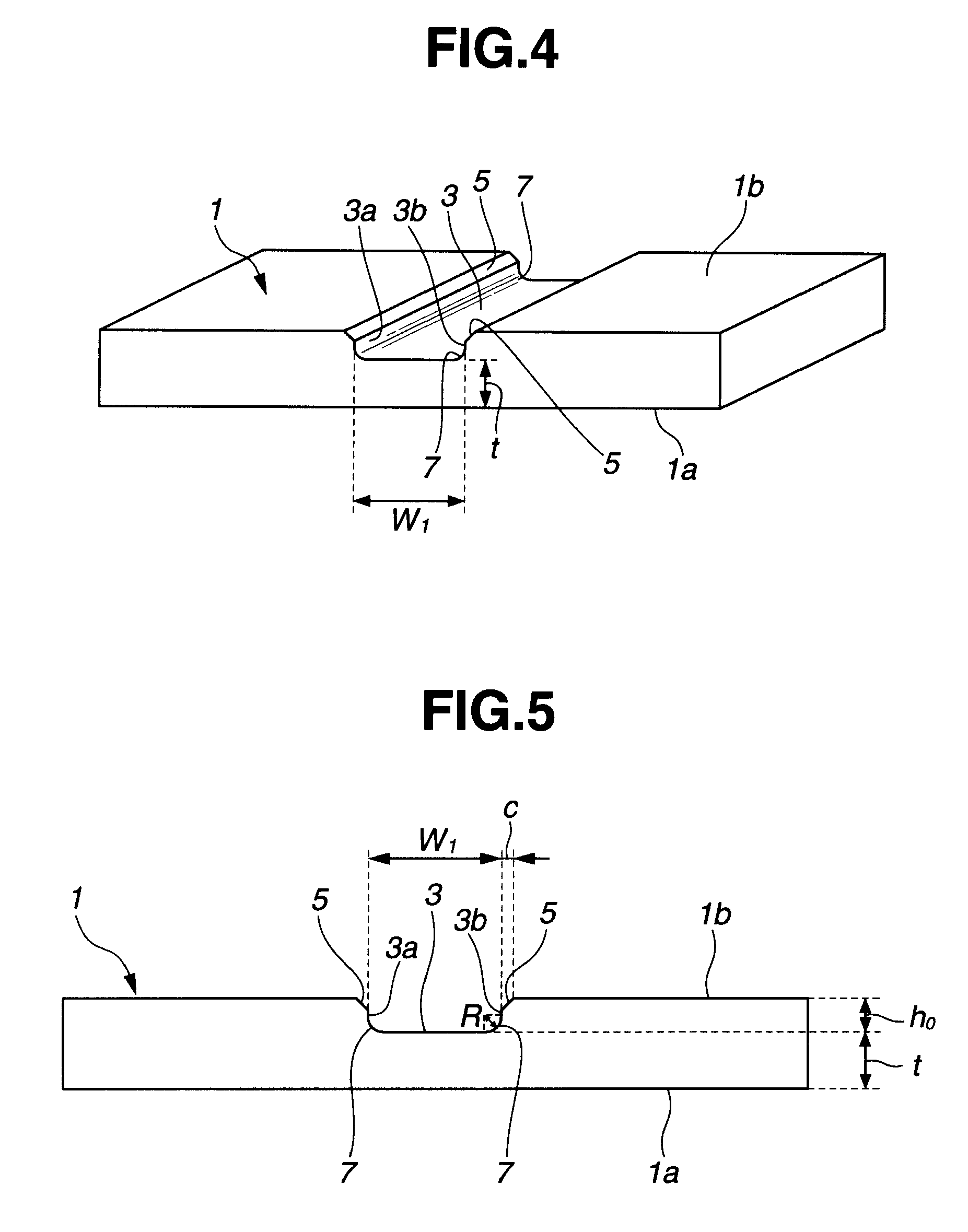
[0097]A synthetic quartz glass substrate B dimensioned 152 mm×152 mm×6.35 mm (thick) having front, back and end surfaces polished to mirror finish was prepared as a starting substrate. Using a machining center and a diamond abrasive wheel, the starting substrate was machined at the center of its back surface to form a channel having a depth of 4.98 mm, a width of 29.9 mm, and a length of 152 mm, extending parallel to the end surface, and having a curvilinear second chamfer with a radius of curvature of 0.9 mm between the channel side and bottom surfaces and a first chamfer with a width of 0.3 mm between the channel side surface and the back surface.

[0098]Next, the machined substrate was fixedly mounted on a platform. A wool felt buff having a diameter of 30 mm and a height of 30 mm adapted to rotate at 1,000 rpm was forced in contact with the bottom surface of the channel under 2,000 Pa and one side wall under 2,000 Pa. The substrate-holding platform was moved back and forth at 50 m...


PUM

PropertyMeasurementUnit
Raaaaaaaaaaa
flatnessaaaaaaaaaa
flatnessaaaaaaaaaa

Abstract

An electronic grade glass substrate is provided with a recess, channel or step in one surface, and a first chamfer between the side surface of the recess, channel or step and the one surface. The side and bottom surfaces of the recess, channel or step are mirror finished, and the first chamfer is mirror finished.

Description

CROSS-REFERENCE TO RELATED APPLICATION[0001]This non-provisional application claims priority under 35 U.S.C. §119(a) on Patent Application No. 2011-232522 filed in Japan on Oct. 24, 2011, the entire contents of which are hereby incorporated by reference.TECHNICAL FIELD[0002]This invention relates to electronic grade glass substrates having a recess, channel or step, and more particularly, to glass substrates for use in the advanced applications of semiconductor-related electronic materials, typically as photomasks, exposure tool components, reticles and nanoimprint molds. It also relates to a method for manufacturing the same.BACKGROUND ART[0003]The quality of electronic grade glass substrates is evaluated in terms of the size and population of defects on the substrate, flatness, surface roughness, photochemical stability of material, and surface chemical stability. The trend toward higher accuracy of the design rule poses ever-tightening requirements on these factors.[0004]Photomas...

Claims


Application Information

Patent Timeline
Patent Type & Authority Patents(United States)
IPC IPC(8): B32B3/00B24B9/06B24B5/50B24B7/22B24B1/00B24B37/02B32B3/02B24B37/04G03F1/60
CPCB24B37/042B24B1/00B24B5/50B24B7/228B24B9/065B24B37/02G03F1/60Y10T428/24355Y10T428/24479B24B9/08B24B37/04H01L23/15
Inventor OKAFUJI, DAIYUYAMAZAKI, HIROYUKITAKEUCHI, MASAKI
Owner SHIN ETSU CHEM IND CO LTD
Why Eureka
Try Eureka