Method of producing encapsulated IC devices on a wafer

Active Publication Date: 2015-12-08
AMERICAN SEMICON
View PDF8 Cites 8 Cited by
  • Summary
  • Abstract
  • Description
  • Claims
  • Application Information

AI Technical Summary

Benefits of technology

[0004]The process of flexible waferscale packaging provides for the assembly of individual die while they are still in waf

Problems solved by technology

However, SoP and conventional semiconductor wafer fabrication fail to make waferscale packaging feasible due to t

Method used


Image

  • Method of producing encapsulated IC devices on a wafer
  • Method of producing encapsulated IC devices on a wafer
  • Method of producing encapsulated IC devices on a wafer

Examples


Embodiment Construction

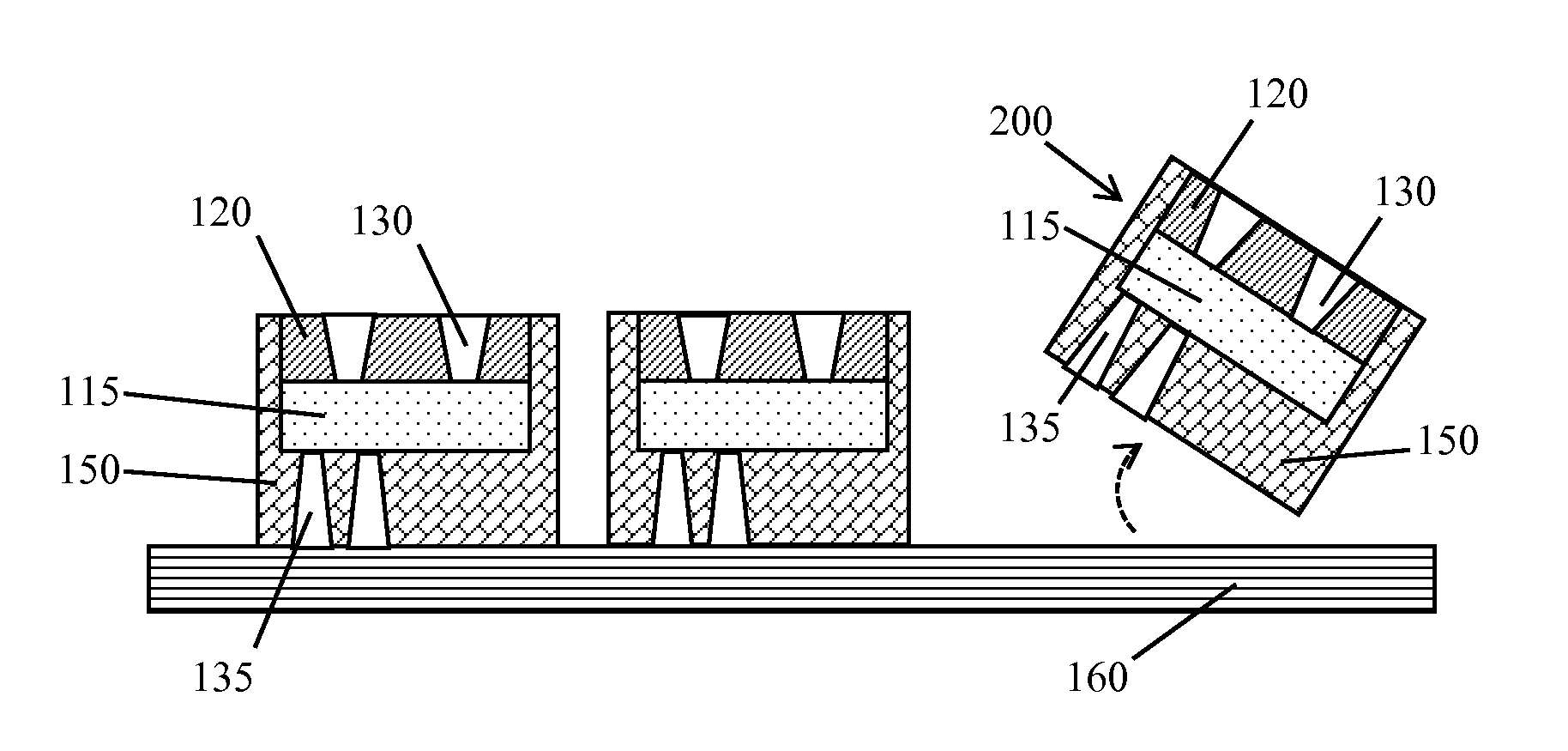
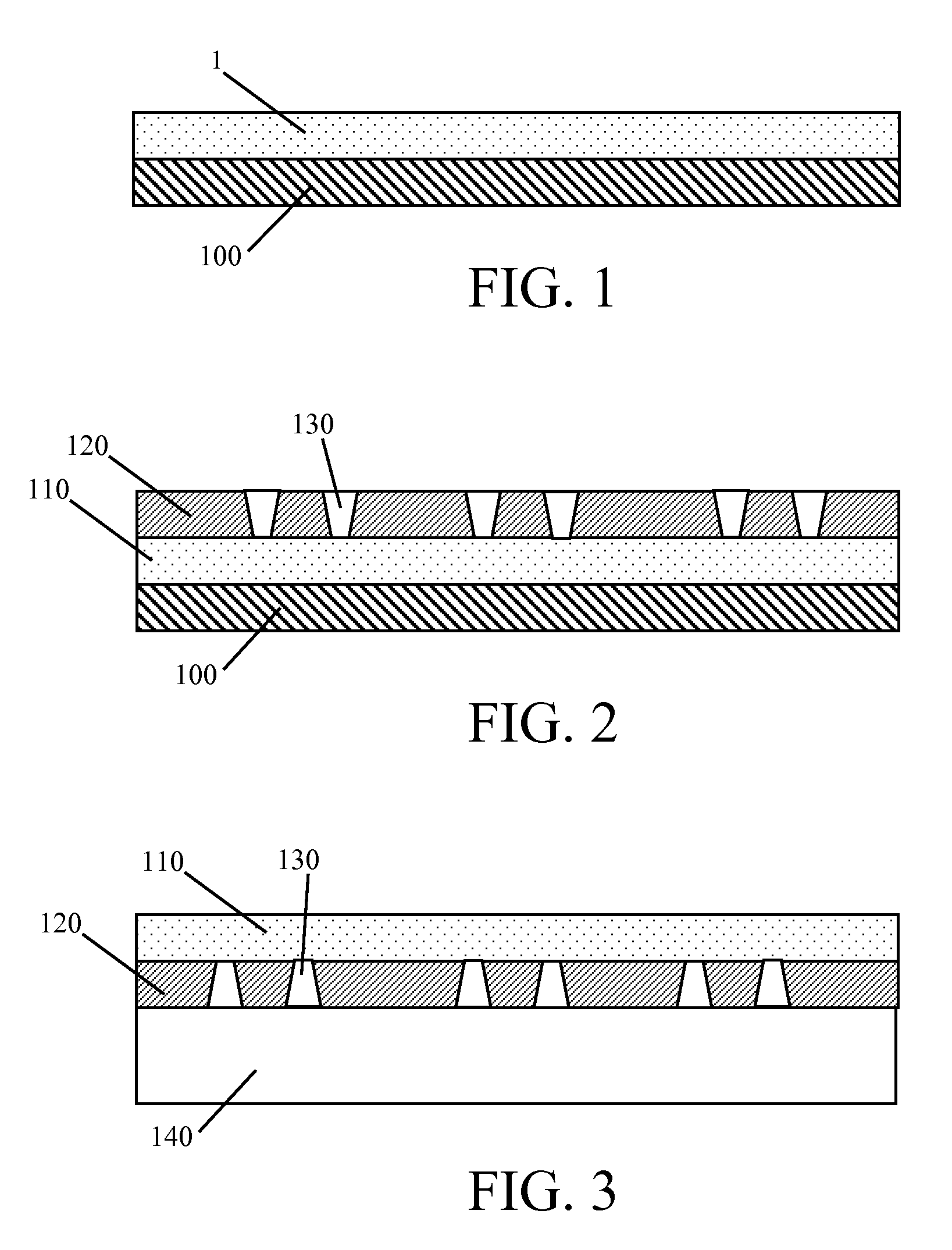
[0029]The Waferscale Packaging (WSP) process described here begins as shown in FIG. 1 with a wafer layer 100. The described processes are well suited to Semiconductor-On-Insulator (SOI) substrates. For the purposes described here, this may be any semiconductor substrate, the most common being silicon or a III-V material such as gallium arsenide (GaAs). A device layer 110, such as CMOS, is applied to or created in the wafer layer 100, an SOI substrate being an example of a device layer created within a wafer layer. Standard semiconductor processing then proceeds to develop the desired Integrated Circuit (IC) devices. Though the illustrations may seem initially to suggest a particular topside versus bottom-side orientation, there is no such intent; it will be seen as the process progresses that it is totally independent of any top-bottom orientation.

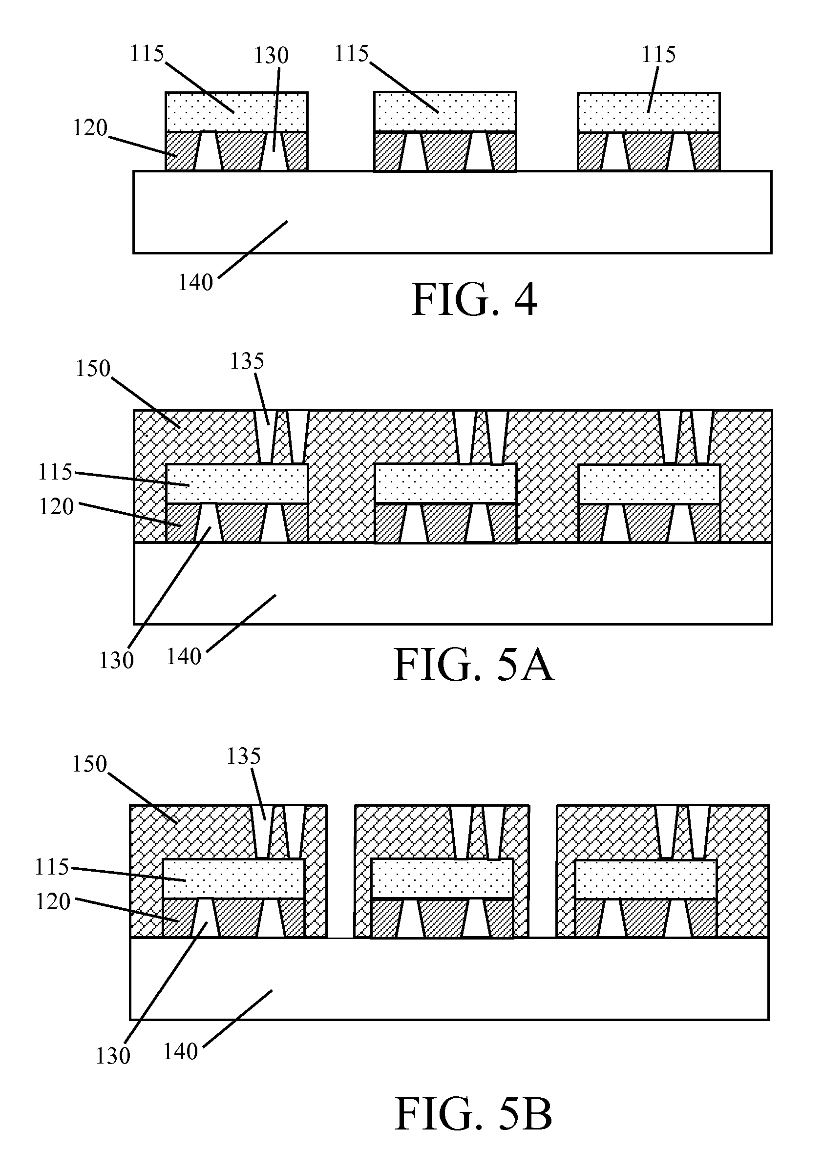
[0030]Following the completion of processing within the device layer 110, it is coated in FIG. 2 with a first polymer 120, such as a poly...


PUM


Abstract

This method of waferscale packaging produces finished integrated circuits (ICs) individually completely encapsulated with environmentally protective packaging material while still in the wafer format. Following conventional semiconductor fabrication of chips at the wafer level and prior to their separation, a first polymer is applied to the front surface of the wafer with allowance for contact holes. A carrier wafer is attached to the exposed polymer. The original substrate is removed and the devices are separated by cutting through the semiconductor layer and the first polymer. A second polymer is applied to cover the exposed backside of the devices and to fill the cut spaces between them, thereby sealing the remaining five surfaces of the chips. The second polymer layer may also include contact holes for access to the back side of the device chips. A second singulation cutting leaves the chips on the wafer prepared for a pick-and-place operation.

Description

CROSS-REFERENCES TO RELATED APPLICATIONS[0001]This application claims benefit of U.S. Provisional Application No. 61 / 808,354 filed Apr. 4, 2013, entitled “Waferscale Packaging”, which is incorporated here by reference in its entirety.FIELD OF THE INVENTION[0002]The present invention relates generally to a method of manufacturing waferscale semiconductor devices. In particular, the described method produces semiconductor devices, flexible or rigid, that are completely encapsulated on the wafer without processing of individual die.BACKGROUND OF THE INVENTION[0003]Assembly of integrated circuits (ICs) is currently completed by thinning the silicon wafer, dicing or singulating the wafer into die, or chips, and then assembling the individual die into a package or applying them individually to a board that will be sealed for protection from the environment.BRIEF SUMMARY OF THE INVENTION[0004]The process of flexible waferscale packaging provides for the assembly of individual die while the...

Claims


Application Information

Patent Timeline
IPC IPC(8): H01L21/56H01L23/31
CPCH01L21/561H01L23/3135H01L21/784H01L21/568H01L24/25H01L21/6835H01L21/6836H01L24/82H01L24/96H01L24/97H01L2221/68327H01L2221/6834H01L2224/04105H01L2224/2518H01L2224/82005H01L2224/94H01L2224/8203H01L21/78H01L2224/03
Inventor HACKLER, SR., DOUGLAS R.WILSON, DALE G.
Owner AMERICAN SEMICON
Why Eureka
Try Eureka