Semiconductor structure and method for manufacturing the same

a technology of semiconductors and semiconductors, applied in the direction of semiconductor devices, electrical equipment, transistors, etc., can solve the problems of short circuit between source and drain, increase the distance between, and the abovementioned two methods still experience defects, so as to effectively suppress short circuits, effectively reduce contact resistance, and reduce the effect of contact resistan

Active Publication Date: 2015-12-08
INST OF MICROELECTRONICS CHINESE ACAD OF SCI
View PDF16 Cites 0 Cited by
  • Summary
  • Abstract
  • Description
  • Claims
  • Application Information

AI Technical Summary

Benefits of technology

[0007]The present invention aims to provide a semiconductor structure and a method for manufacturing the same, which can effectively reduce contact resistance at source / drain regions at the mean time of guaranteeing performance of semiconductor structures.
[0021]As compared to the prior art, the present invention exhibits following advantages: with regard to a semiconductor structure with very thin source / drain regions, in particular, an ultra-thin SOI structure and a semiconductor structure having fins, the present invention proposes to form very thin first contact layers on surfaces of source / drain regions through self-limited process, then to form amorphous semiconductor layers on surfaces of source / drain regions, and then to form second contact layers on surfaces of the amorphous semiconductor layers through self-limited process. Formation of the thin first contact layers prevents semiconductor at source / drain regions from being depleted completely, thereby effectively suppressing short-circuits to occur between source and drain. Besides, owing to presence of amorphous semiconductor layers and second contact layers, contact resistance at source / drain regions can be reduced effectively. Therefore, the present invention can effectively reduce contact resistance at source / drain regions along with guaranteeing performance of semiconductor structures.

Problems solved by technology

However, when aforesaid method is used to form metal silicide layers in the case source / drain regions are quite thin, for example, the semiconductor structure is ultra-thin SOI or finFET, silicon in source / drain regions would be easily depleted completely, and even silicon under sidewall spacers of a gate stack would be depleted as well during formation of metal silicide layers, which consequently leads to problems like silicide piping and further causes short-circuits between source and drain, during formation of metal silicide layers.
However, abovementioned two methods still experience some defects.
Although silicon in source / drain regions is saved from being depleted completely through increasing thickness of source / drain regions by means of RSD method, this also increases distance between metal silicide layers and channels at the meantime, thereby hindering performance of semiconductor devices.
Likewise, although the metal silicide layers formed on surfaces of source / drain regions by means of self-limited process are quite thin, their lateral electrical resistance is rather great, which impairs performance of semiconductor devices as well.

Method used


Image

  • Semiconductor structure and method for manufacturing the same
  • Semiconductor structure and method for manufacturing the same
  • Semiconductor structure and method for manufacturing the same

Examples


Embodiment Construction

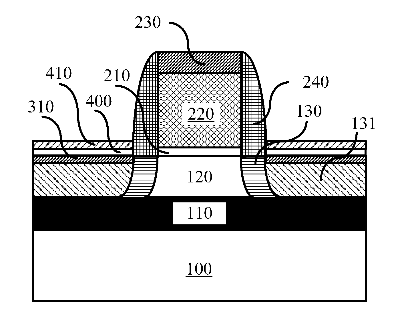
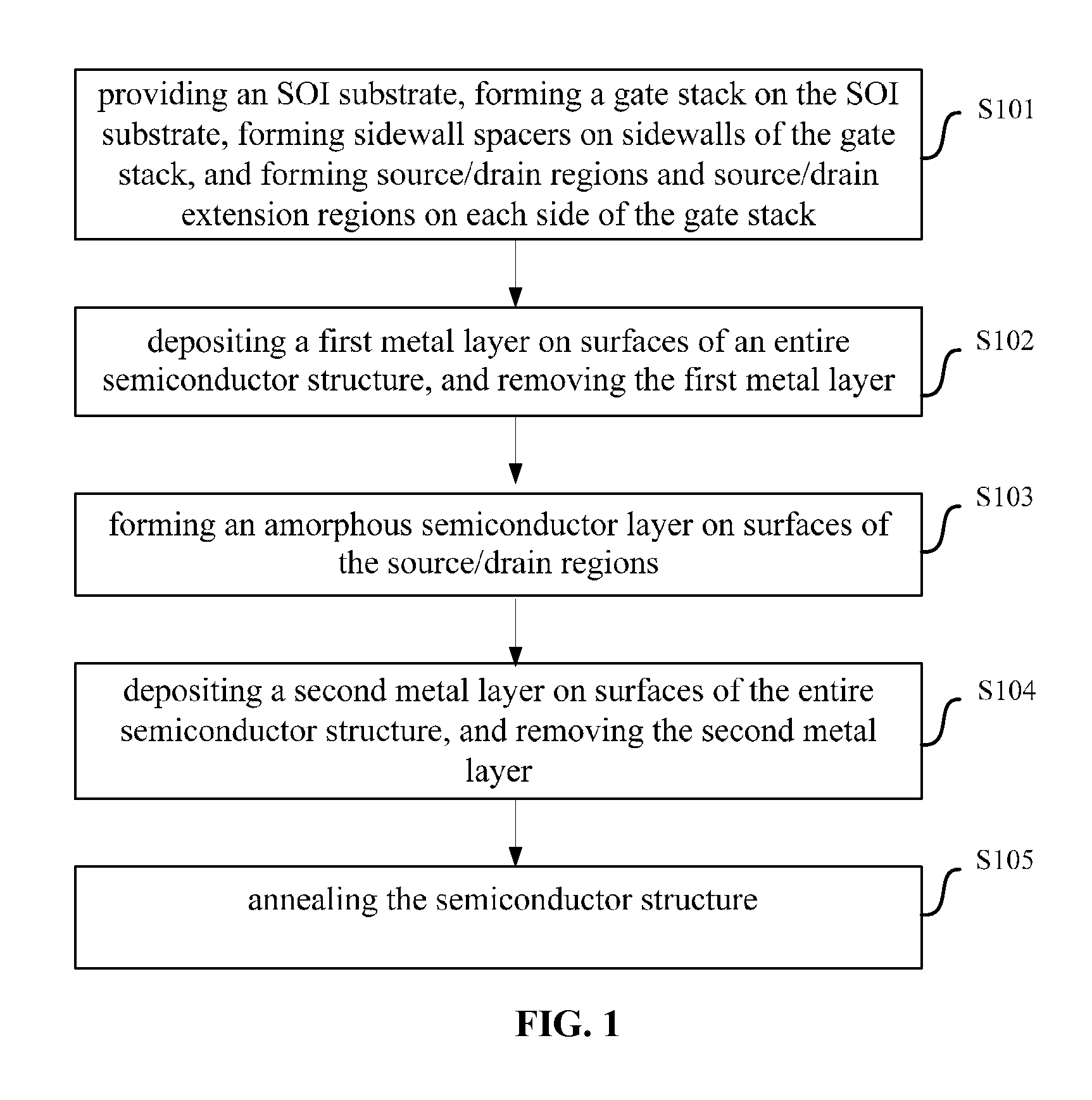
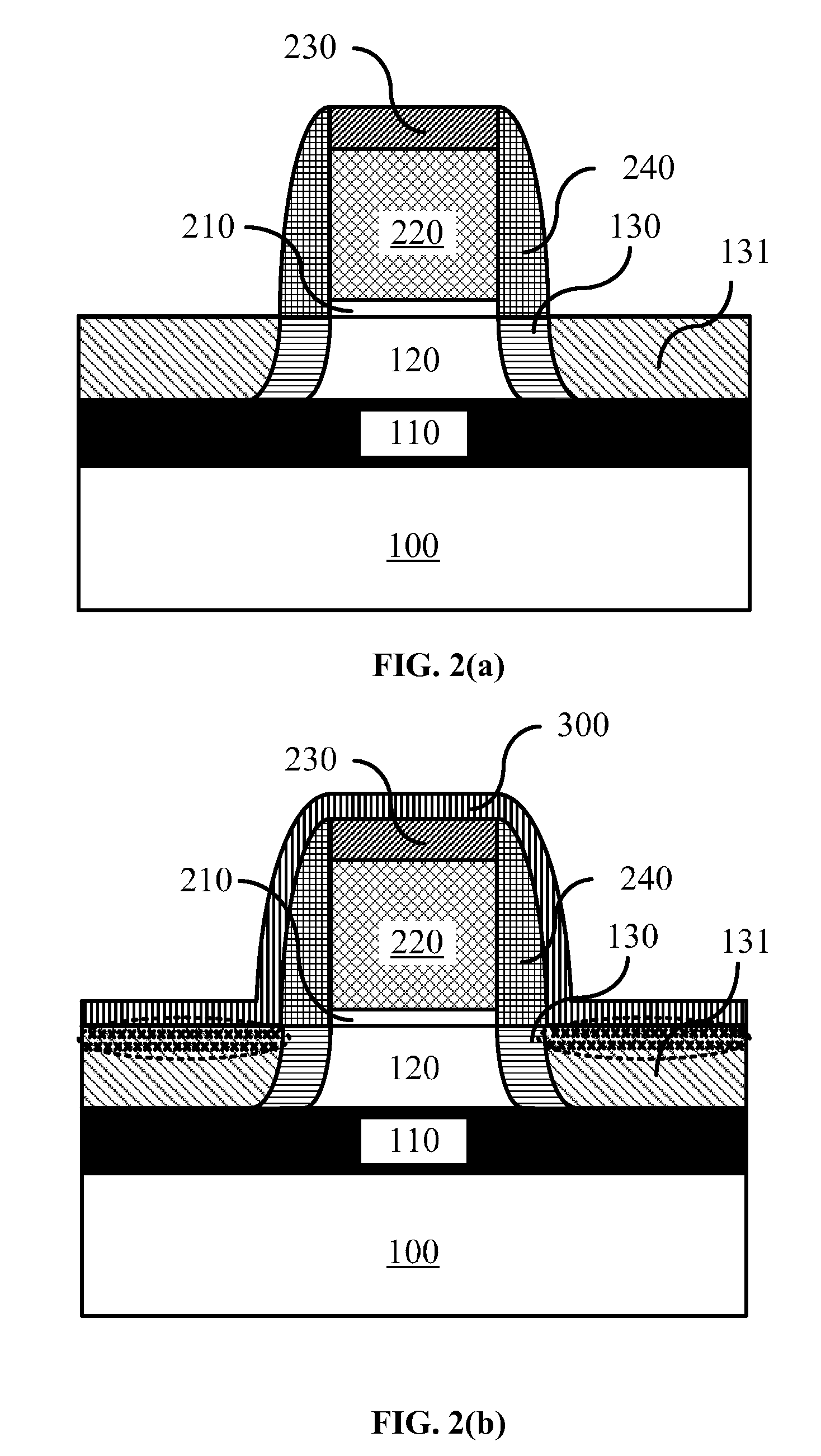
[0025]Embodiments of the present invention are described in detail here below, wherein examples of the embodiments are illustrated in the drawings. It should be appreciated that the embodiments described below in conjunction with the drawings are illustrative and are provided for explaining the prevent invention only, thus shall not be interpreted as limitations to the present invention.

[0026]Various embodiments or examples are provided here below to implement different structures of the present invention. To simplify disclosure of the present invention, description of components and arrangements of specific examples is given below. Of course, they are illustrative only and not limiting the present invention. Moreover, in the present invention, reference numbers and / or letters may be repeated in different embodiments. Such repetition is for purposes of simplicity and clarity, yet does not denote any relationship between respective embodiments and / or arrangements being discussed. Fur...


PUM


Abstract

A method for manufacturing a semiconductor structure comprises following steps: providing an SOI substrate, forming a gate stack on the SOI substrate, forming sidewall spacers on sidewalls of the gate stack, and forming source / drain regions on each side of the gate stack; depositing a first metal layer on surfaces of an entire semiconductor structure, and then removing the first metal layer; forming an amorphous semiconductor layer on surfaces of the source / drain regions; depositing a second metal layer on surfaces of the entire semiconductor structure, and then removing the second metal layer; and annealing the semiconductor structure. Accordingly, the present invention further provides a semiconductor structure. The present invention is capable of effectively reducing contact resistance at source / drain regions.

Description

CROSS REFERENCE TO RELATED APPLICATION[0001]This application is a national stage application, filed under 35 U.S.C. §371, of PCT Application No. PCT / CN2011 / 083329, filed on Dec. 1, 2011, entitled “SEMICONDUCTOR STRUCTURE AND METHOD FOR MANUFACTURING THE SAME”, which claimed priority to Chinese Application No. 201110375108.5, filed on Nov. 23, 2011, all of which are hereby incorporated by reference in their entirety.FIELD OF THE INVENTION[0002]The present invention relates to semiconductor manufacturing field, particularly, to a semiconductor structure and a method for manufacturing the same.BACKGROUND OF THE INVENTION[0003]One of methods usually used to reduce contact resistance at source / drain regions of a semiconductor structure is to form contact layers (which are usually metal silicide layers; accordingly, metal silicide layers are exemplified as contact layers hereinafter) on surfaces of source / drain regions. Namely, metal layers are deposited on surfaces of source / drain region...

Claims


Application Information

Patent Timeline
Patent Type & Authority Patents(United States)
IPC IPC(8): H01L27/12H01L29/45H01L29/66H01L29/786H01L21/285H01L21/324
CPCH01L29/665H01L21/28518H01L21/324H01L29/458H01L29/66772H01L29/78603H01L29/78618
Inventor YIN, HAIZHOUXU, JINGLIU, YUNFEI
Owner INST OF MICROELECTRONICS CHINESE ACAD OF SCI
Why Eureka
Try Eureka