Liquid crystal display device

a display device and liquid crystal technology, applied in static indicating devices, non-linear optics, instruments, etc., can solve problems such as problems such as problems in displaying images, and achieve the effects of improving the viewing angle dependency of gamma characteristics, high display quality, and increasing the aperture ratio in each pixel

Active Publication Date: 2016-01-05
SHARP KK
View PDF6 Cites 2 Cited by
  • Summary
  • Abstract
  • Description
  • Claims
  • Application Information

AI Technical Summary

Benefits of technology

[0035]According to the present invention, a plurality of common electrodes are provided for each pixel, and different potentials are supplied to the respective common electrodes in each pixel, thereby driving the liquid crystal layer separately for each of the common electrodes in each pixel. This makes it possible to improve the viewing angle dependency of the gamma characteristics without dividing each pixel electrode, and because it is not necessary to provide each pixel with at least twice as many switching elements and storage capacitance elements as the normal structure, the aperture ratio in each pixel can be increased as compared with the conventional pixel division structure. As a result, it is possible to provide a liquid crystal display device that has high display quality and that can display a bright image with low power consumption.

Problems solved by technology

If the gamma characteristics differ between the front direction and the diagonal direction, the gradation display state also differs depending on the viewing direction, resulting in a problem in displaying images.

Method used


Image

  • Liquid crystal display device
  • Liquid crystal display device
  • Liquid crystal display device

Examples


embodiment 1

[0068]In Embodiment 1, a transmissive liquid crystal display device S of a TFT type will be explained as an example of an active matrix driving liquid crystal display device.

[0069]—Configuration of Liquid Crystal Display Device S—

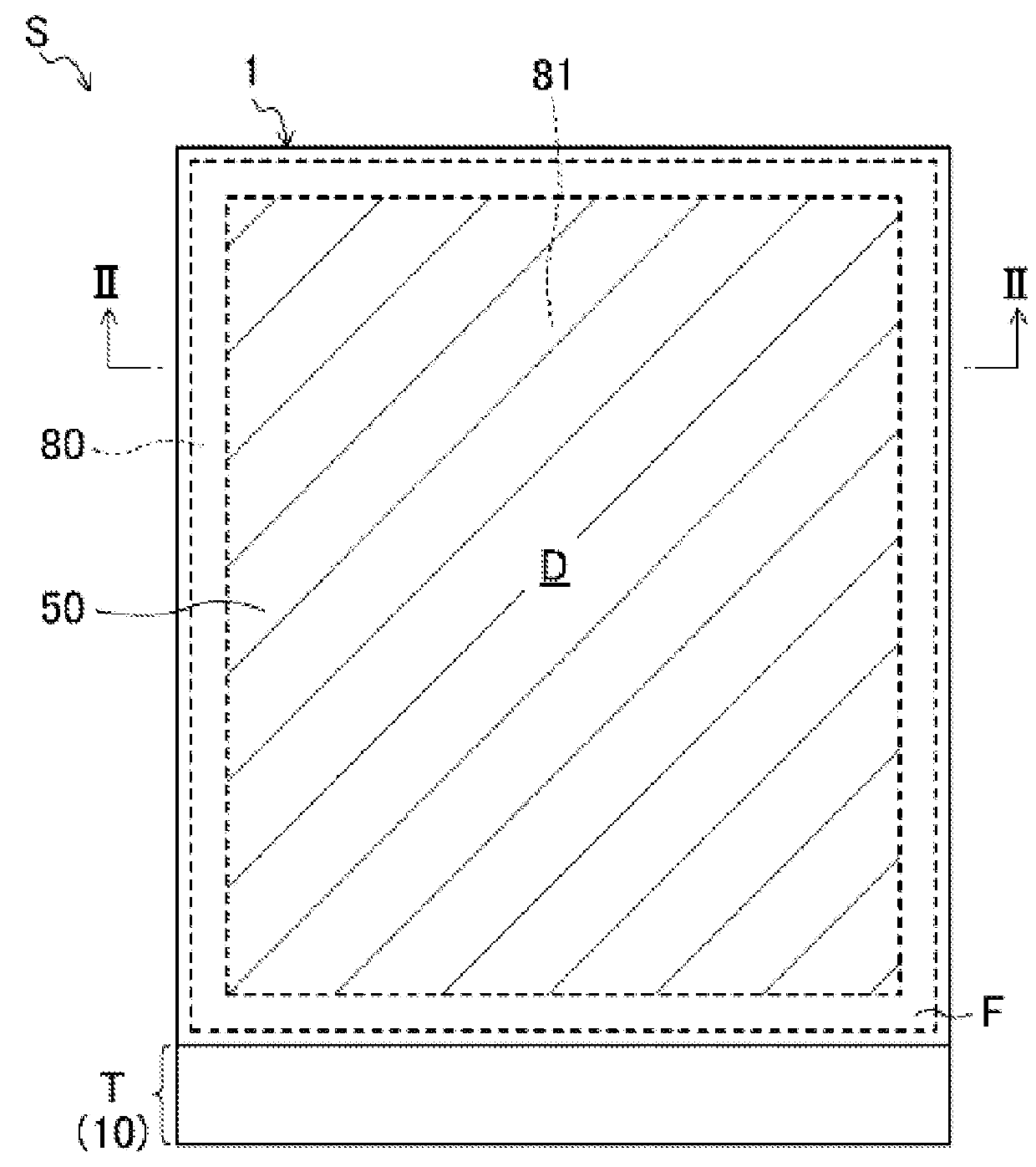
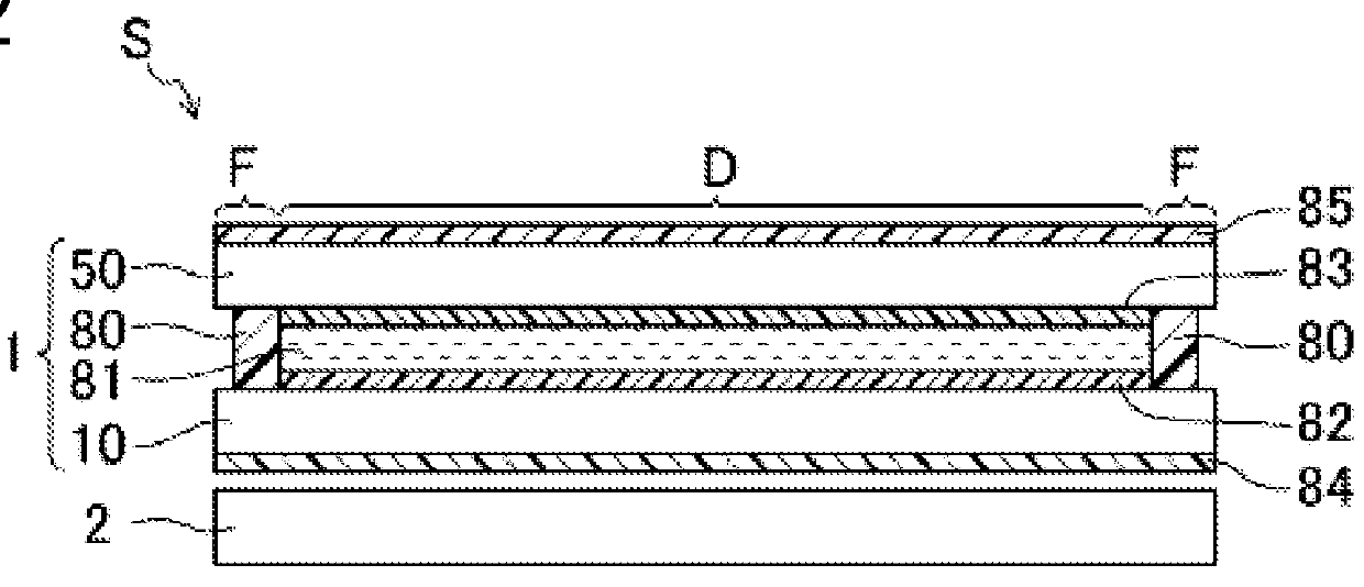
[0070]The configuration of the liquid crystal display device S is shown in FIGS. 1 and 2. FIG. 1 is a schematic plan view of the liquid crystal display device S. FIG. 2 is a schematic cross-sectional view showing a cross-sectional structure along the line II-II of FIG. 1. A polarizing plate 85 shown in FIG. 2 is not shown in FIG. 1.

[0071]The liquid crystal display device S includes a flat plate-shaped thin liquid crystal display panel 1 and a backlight unit 2 disposed on the rear side of the liquid crystal display panel 1.

[0072]1>

[0073]The liquid crystal display panel 1 includes an array substrate 10 and an opposite substrate 50 disposed to face each other, a frame-shaped sealing member 80 that bonds respective outer edges of the array substrate 10 and the ...

modification example 1 of embodiment 1

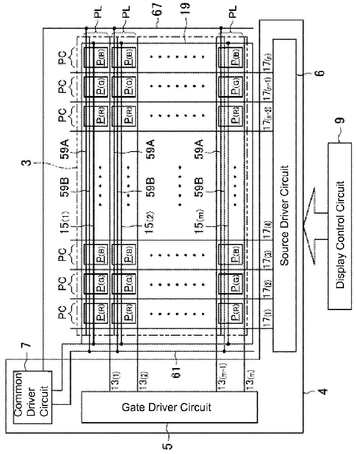
[0179]In Embodiment 1, the gate driver circuit 5 and the source driver circuit 6 were configured to conduct the dot inversion driving, but in this modification example, the gate driver circuit 5 and the source driver circuit 6 are configured to conduct V line inversion driving (column inversion driving) in which, in one display frame, polarities of data potentials supplied to the respective pixel electrodes 41 are inverted for every pixel column PC, based on the display signals inputted from the display control circuit 9.

[0180]FIG. 11 shows a schematic plan view showing an arrangement of bright subpixels (bright regions) and dark subpixels (dark regions) of the respective pixels P in one display frame in a display operation of the liquid crystal display device S in which the V line inversion driving and the common inversion driving are combined.

[0181]In the liquid crystal display device S of this modification example, in one display frame, different common potentials are respectivel...

modification example 2 of embodiment 1

[0184]In this modification example, the gate driver circuit 5 and the source driver circuit 6 are configured to conduct H line inversion driving (row inversion driving) in which, in one display frame, polarities of data potentials supplied to the respective pixel electrodes 41 are inverted for every pixel row PL, based on the display signals inputted from the display control circuit 9.

[0185]Although not shown in the figure, the second common electrodes 59B in alternate pixel rows PL, or in other words, the second common electrodes 59B in odd-numbered pixel rows PL and the second common electrodes 59B in even-numbered pixel rows PL, are connected to different second common wiring lines 67 respectively extend along one side of the frame region F, and are thereby connected to different second terminals 71.

[0186]The led-out portions of the second common electrodes 59B in the odd-numbered rows and the second common wiring line 67 to which the respective second common electrodes 59B in th...


PUM

PropertyMeasurementUnit
thickaaaaaaaaaa
thickaaaaaaaaaa
thickaaaaaaaaaa

Abstract

A liquid crystal display device of the present invention is provided with: an array substrate (10) in which a pixel electrode (41), a TFT (20), and a storage capacitor element (30) are provided for each pixel (P); an opposite substrate (50) in which a plurality of common electrodes (59A, 59B) are provided for each pixel (P); a liquid crystal layer (81); and a driver circuit (4) that dividedly drives the liquid crystal layer (81) of each pixel (P) through each of the common electrodes (59A, 59B) by supplying a predetermined potential to each pixel electrode (41) and supplying different potentials to the respective common electrodes (59A, 59B) in each pixel (P). The liquid crystal display device according to the present invention has improved viewing angle dependency of the gamma characteristics, while increasing the aperture ratio of each pixel.

Description

TECHNICAL FIELD[0001]The present invention relates to a liquid crystal display device, and in particular, to a countermeasure for improving both the viewing angle dependency of gamma characteristics and the pixel aperture ratio.BACKGROUND ART[0002]It has been known that, in a liquid crystal display device, gamma characteristics have a viewing angle dependency, and as a technology to address this problem, a pixel division structure (also referred to as a multi-pixel structure) is proposed. The gamma characteristics mean a gradation dependency of the display brightness. If the gamma characteristics differ between the front direction and the diagonal direction, the gradation display state also differs depending on the viewing direction, resulting in a problem in displaying images.[0003]In a liquid crystal display device having the pixel division structure, each pixel is constituted of two subpixels, and each pixel electrode is divided into two subpixel electrodes corresponding to the s...

Claims


Application Information

Patent Timeline
Patent Type & Authority Patents(United States)
IPC IPC(8): G09G3/36G02F1/1343G02F1/1362
CPCG02F1/134363G02F1/136213G09G3/3655G02F2001/134318G02F2001/134345G09G2300/0426G09G2300/0447G09G2300/0452G09G2300/0465G09G2300/0876G09G2320/028G02F1/134318G02F1/134345
Inventor UCHIDA, SEIICHI
Owner SHARP KK
Why Eureka
Try Eureka