Semiconductor device and method for forming the same

a semiconductor device and a technology of a semiconductor device, applied in the direction of semiconductor devices, semiconductor/solid-state device details, electrical devices, etc., can solve the problems of deformation of an internal portion of the semiconductor device, the increase of the number of stacked conductive layers, and the increase of the device's precision and complexity, so as to reduce the occurrence of cracks, reduce or prevent the occurrence of defects, and increase the design rule margin

Active Publication Date: 2016-02-09
SK HYNIX INC
View PDF15 Cites 8 Cited by
  • Summary
  • Abstract
  • Description
  • Claims
  • Application Information

AI Technical Summary

Benefits of technology

[0005]Embodiments of the present disclosure relate to a semiconductor device and a method of forming the same that reduce the occurrence of a crack in a portion of a pad region. Embodiments of the present disclosure also relate to increasing the design rule margin between pad regions.
[0006]Embodiments of the present disclosure relate to a semiconductor device and a method for forming the same that reduces or prevents the occurrence of a defect (e.g., a crack or void) in a MOS capacitor or a circuit, which are disposed at a lower part of the pad region. Embodiments are also directed to improving device characteristics by increasing a design rule margin between pad regions.

Problems solved by technology

The number of stacked conductive layers increases as these semiconductor devices become more precise and complicated.
The machine exerts force on the bonding pad and causes deformation of an internal portion of the semiconductor device.
In addition, as the degree of integration increases, the size of a region between two neighboring pad regions is reduced, and it becomes more difficult to form one or more conductive lines between the pad regions.

Method used


Image

  • Semiconductor device and method for forming the same
  • Semiconductor device and method for forming the same
  • Semiconductor device and method for forming the same

Examples


Embodiment Construction

[0031]Reference will now be made in detail to embodiments, some of which are illustrated in the accompanying drawings. Wherever possible, the same reference numbers are used throughout the drawings to refer to the same or like portions. A semiconductor device and a method for forming the same according to embodiments will hereinafter be described with reference to the accompanying drawings.

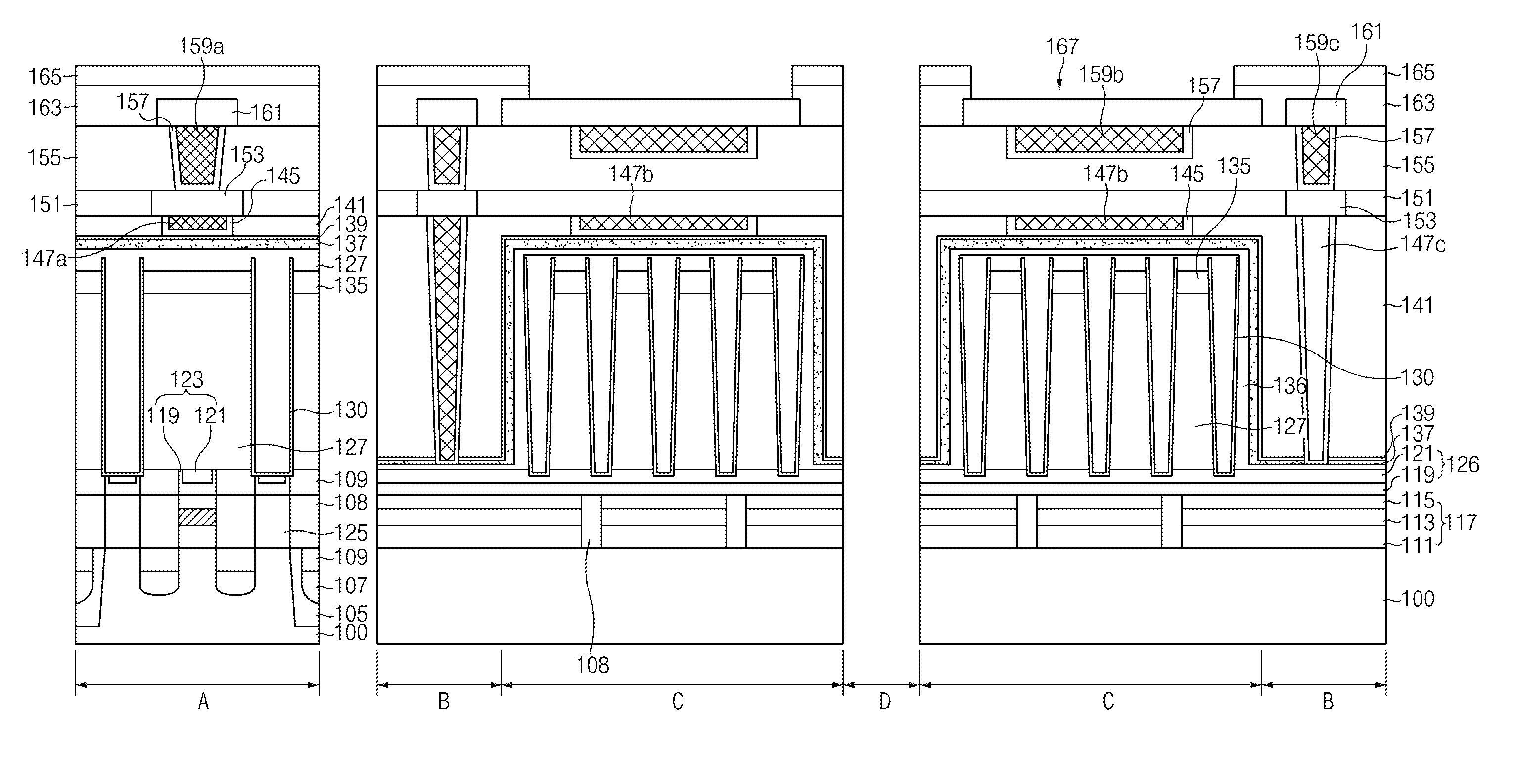
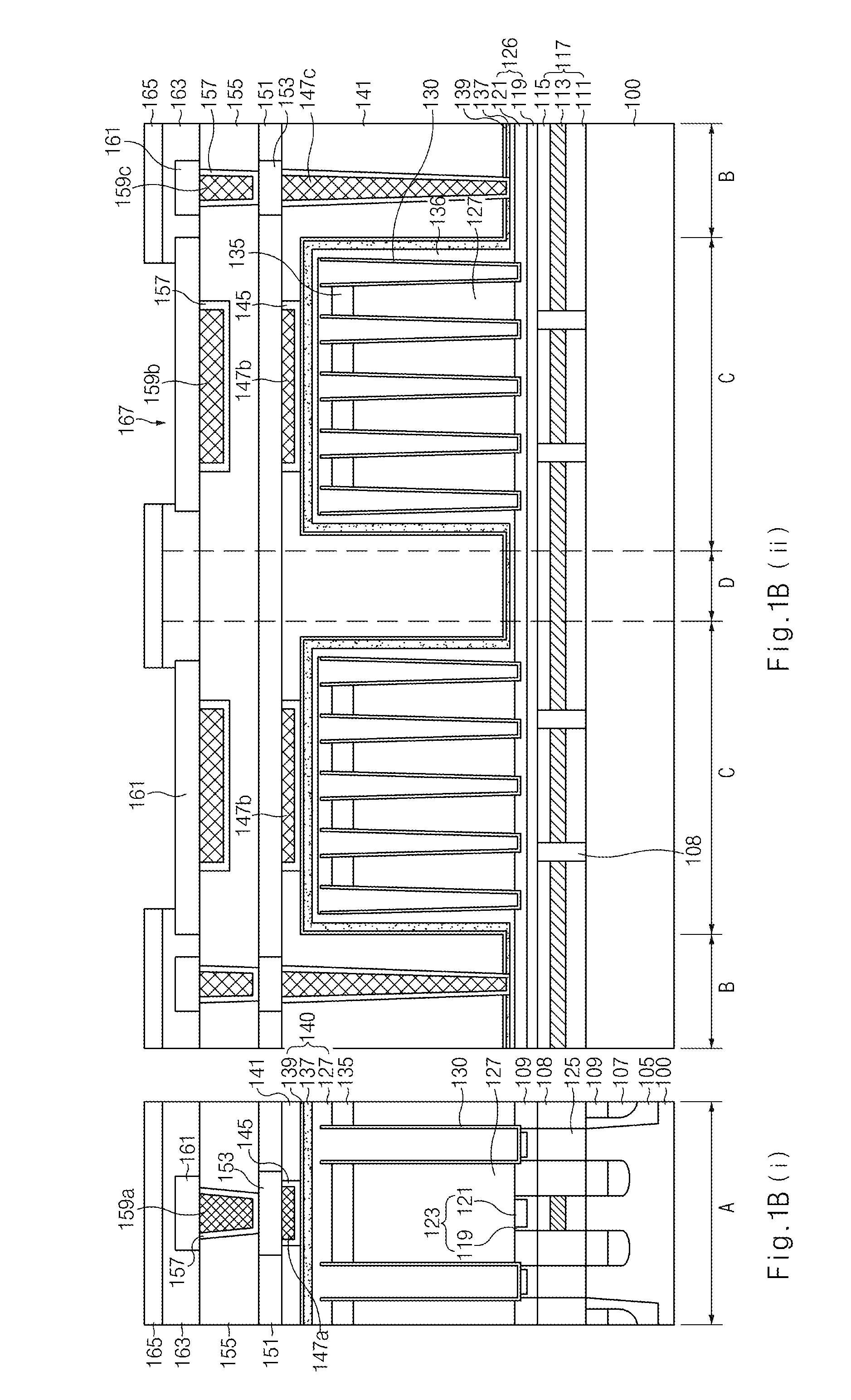
[0032]FIGS. 1A and 1B are plan views and cross-sectional views illustrating a semiconductor device according to an embodiment.

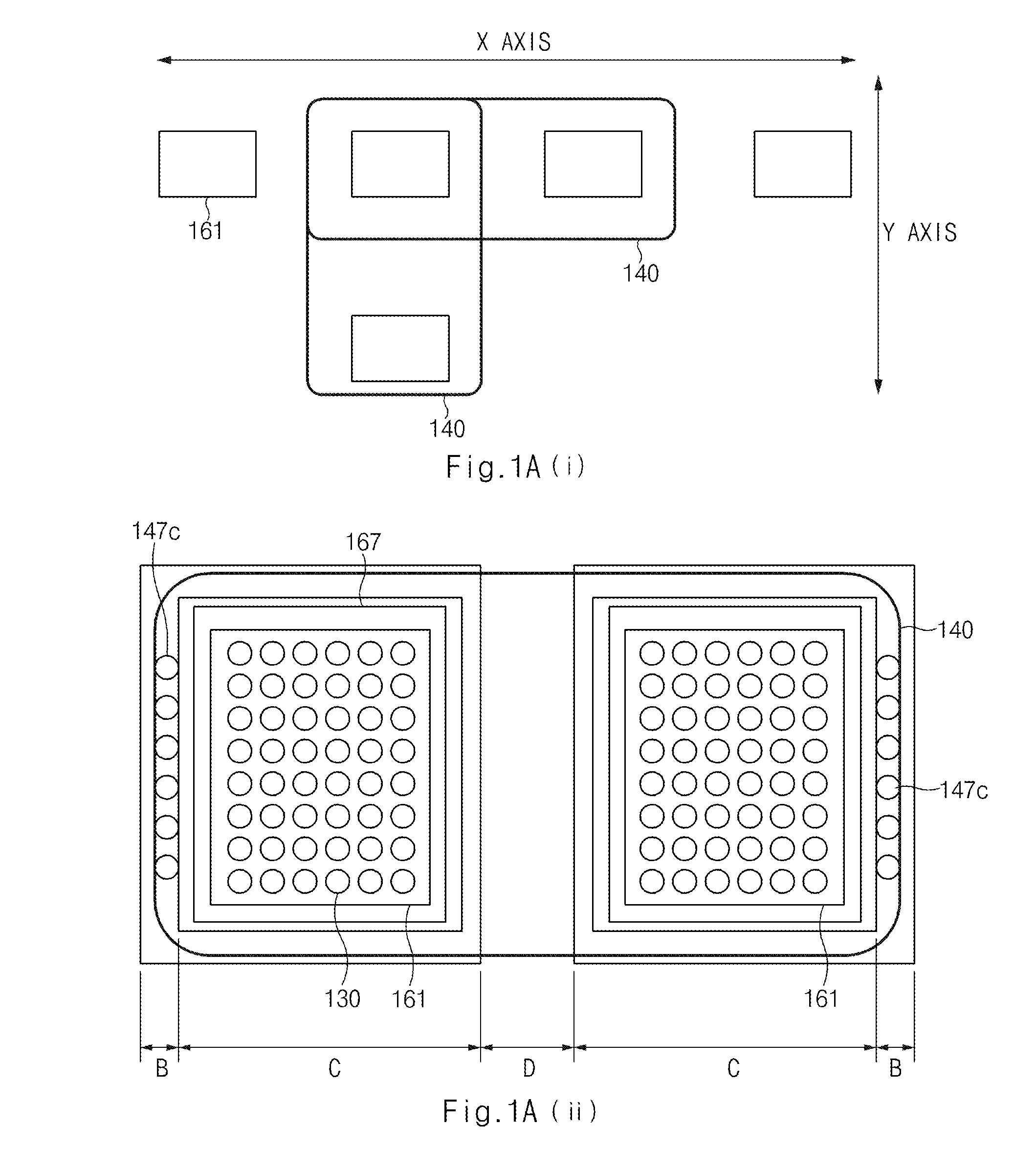
[0033]Referring to FIG. 1A(i), a plurality of metal pads 161 are arranged in a direction along an X-axis (hereinafter, “an X-axis direction”) and in a direction along a Y-axis (hereinafter, “a Y-axis direction”).

[0034]FIG. 1A(ii) is an enlarged view illustrating a portion of the semiconductor device shown in FIG. 1A(i), which includes two metal pads 161. A peripheral region B is located at one side of each pad region C, and a coupling portion D is disposed between neighbori...


PUM


Abstract

A semiconductor device includes a first pad region including a plurality of first storage nodes, a second pad region neighboring the first pad region and including a plurality of second storage nodes, a coupling portion disposed between the first pad region and the second pad region, and a plate electrode disposed over the plurality of first storage nodes of the first pad region and the plurality of second storage nodes of the second pad region, and disposed in the coupling portion to interconnect the first pad region and the second pad region.

Description

CROSS-REFERENCE TO RELATED APPLICATION[0001]Priority to Korean patent application No. 10-2014-0030355, filed on 14 Mar. 2014, the disclosure of which is hereby incorporated in its entirety by reference, is claimed.BACKGROUND[0002]Generally, highly-integrated semiconductor devices have been formed by stacking conductive layers (for example, a conductive layer including a metal film and an insulation layer), and by interconnecting stacked conductive layers. The number of stacked conductive layers increases as these semiconductor devices become more precise and complicated. After the desired number of conductive layers are stacked, a bonding pad having a multi-layer structure that includes a plurality of conductive films is formed.[0003]The bonding pad has a line structure disposed over a surface of the integrated circuit and is configured to provide a contact surface between an external pin lead and an internal circuit of the semiconductor device. A bonding wire provides an electrical...

Claims


Application Information

Patent Timeline
Patent Type & Authority Patents(United States)
IPC IPC(8): H01L23/00H01L29/423H01L27/088
CPCH01L24/05H01L23/562H01L27/088H01L29/4236H01L2224/04042H01L2224/05083H01L2224/05184H01L2924/01014H01L2924/01032H01L2924/0484H01L2924/04941H01L2924/13091H01L2924/1436H01L2924/1443H01L24/03H01L2224/02235H01L2224/0391H01L2224/0392H01L2224/05567H01L2224/05624H01L2924/3512H01L2924/00014
Inventor KIM, JUNG, SAM
Owner SK HYNIX INC
Why Eureka
Try Eureka