
Plasma processing apparatus

a plasma processing apparatus and plasma technology, applied in the direction of chemical vapor deposition coating, coating, electric discharge tube, etc., can solve the problems of insufficient study of passive antenna operation, inability to meet the diverse and high-degree of process performance required by a recent plasma processing apparatus, and inability to accurately control the plasma density distribution. , to suppress the wavelength

Active Publication Date: 2016-03-22
TOKYO ELECTRON LTD
View PDF16 Cites 14 Cited by
  • Summary
  • Abstract
  • Description
  • Claims
  • Application Information

AI Technical Summary

Benefits of technology

[0014]In view of the foregoing, illustrative embodiments provide an inductively coupled plasma processing apparatus capable of accurately controlling a plasma density distribution as desired by using a coil in an electrically floating state while suppressing a wavelength effect within a RF antenna.
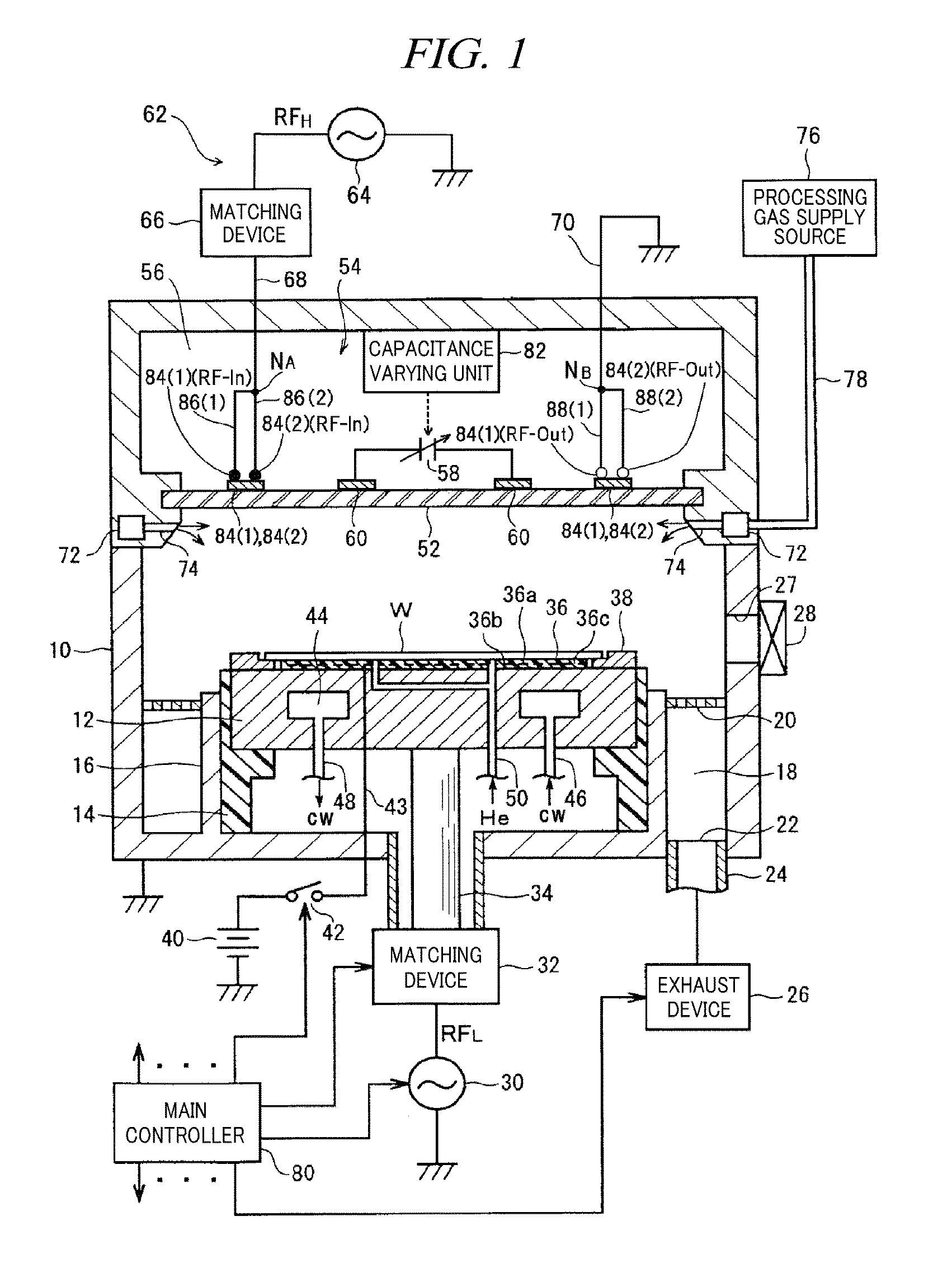
[0016]In accordance with the plasma processing apparatus of the illustrative embodiment, when the high frequency power is supplied from the high frequency power supply unit to the RF antenna, a RF magnetic field is generated around a conductor of the RF antenna by a high frequency current flowing in the RF antenna, and an induced electric field is generated in the processing chamber by the high frequency electric discharge of the processing gas. Herein, since the RF antenna includes a multiple number of coil segments connected electrically in parallel to one another, a wavelength effect within the RF antenna and a voltage drop depend on a length of the coil segments. Therefore, the coil segment number or the coil segment length within each coil is set so as to prevent the wavelength effect from occurring within the individual coil segments and also so as to prevent the voltage drop from being increased. Regarding a magnetomotive force within the RF antenna, a self-inductance of coil segments of each coil is set to be substantially equal to one another, so that a regular or uniform high frequency current flows in the circumferential direction of the coil. Thus, it is possible to constantly obtain a uniform plasma density distribution in the circumferential direction.
[0020]By using the floating coil having the capacitor, it is possible to variously control the plasma density distribution in the donut-shaped plasma in the radial direction as desired. Accordingly, it is possible to accurately control the plasma density distribution around the substrate on the substrate holding unit as desired, and it is possible to increase uniformity of a plasma process.
[0026]By using the floating coil having the capacitor, it is possible to variously control the plasma density distribution in the donut-shaped plasma in the radial direction as desired. Accordingly, it is possible to accurately control the plasma density distribution around the substrate on the substrate holding unit as desired, and it is possible to increase uniformity of a plasma process.
[0027]In accordance with the plasma processing apparatus of the illustrative embodiment, in an inductively coupled plasma processing apparatus, it is possible to accurately control the plasma density distribution as desired by using the coil in an electrically floating state while suppressing the wavelength effect within the RF antenna by the above-described configuration and operation.

Problems solved by technology

However, only with a conventional RF antenna, the plasma density on the substrate is not sufficiently uniform for most plasma processes.
In the inductively coupled plasma processing apparatus, it is also one of the important issues to improve uniformity of the plasma density on the substrate since a uniformity / reproducibility and a production yield of a plasma process depend on the uniformity of the plasma density.
However, since an operation of the passive antenna is not sufficiently studied and verified, a specific apparatus configuration capable of accurately controlling the plasma density distribution as desired by using the passive antenna is not suggested.
Therefore, if a magnetic field of the RF antenna (inductive antenna) is not controlled so as to maintain uniformity of a plasma process on the substrate even when a processing condition of a process recipe is changed, it is not possible to satisfy diverse and high-degree of process performances required by a recent plasma processing apparatus.
If the wavelength effect occurs, it may be difficult to achieve uniformity of plasma density distribution in a radial direction as well as in a circumferential direction.

Method used


Image

  • Plasma processing apparatus
  • Plasma processing apparatus
  • Plasma processing apparatus

Examples


example 1

[Example 1 of Configuration of Floating Coil]

[0161]Hereinafter, when a commercially available capacitor is used as the variable capacitor 58, configuration examples of the variable capacitor 58 in the floating coil 60 of the inductively coupled plasma processing apparatus of the illustrative embodiments will be explained with reference to FIGS. 11 to 15.

[0162]In the example illustrated in FIG. 11, the gap G60 is formed at the floating coil 60, and a commercially available two-terminal capacitor 58 is provided at a position of the gap. In this example, capacitor connection conductors 100a and 100b that connect the coil conductor of the floating coil 60 with a terminal of a package main body of the capacitor 58 are stood uprightly from (desirably, uprightly above) the coil conductor.

[0163]As described above, when a high induced current IIND flows in the floating coil 60, a large-sized variable capacitor 58 that allows a high current to pass is used. However, as the size of the capacit...

example 2

[Example 2 of Configuration of Floating Coil]

[0174]Hereinafter, referring to FIGS. 16 to 18, there will be explained an example in which the variable capacitor 58 as a structure is provided at the floating coil 60 as a part thereof.

[0175]As depicted in FIG. 16, in this example, plate-shaped or sheet-shaped dielectric member 108 and fixed contact conductor 110 having the same thickness are fixed on a coil conductor end 60a adjacent to the gap G60. Herein, the fixed contact conductor 110 is positioned farther from the gap G60 than the dielectric member 108. A plate-shaped or sheet-shaped fixed contact conductor 112 having the same thickness is fixed on the other coil conductor end 60b adjacent to the gap G60 on the opposite side. A movable electrode 114 is configured to slidably move on upper surfaces of the fixed contact conductor 110, dielectric member 108, and fixed contact conductor 112 arranged in a plane so as to move along the circumferential direction. The circumferential dire...

modification example

Another Illustrative Embodiment or Modification Example

[0230]A loop shape of a coil of a RF antenna in accordance with the present illustrative embodiments is not limited to a circular shape. Although not illustrated, it may be a square shape or a triangular shape. Further, a multiple number of coil segments of each antenna coil (loop) may have a different shape and different self-impedance to one another.

[0231]In the present illustrative embodiments, an impedance control unit of the RF antenna is not limited to a fixed capacitor or a variable capacitor as described above. By way of example, it may be a coil or an inductor or a unit including a capacitor and an inductor and may also include a resistance component.

[0232]FIG. 47 illustrates a configuration example in which a transformer 160 is provided between the matching device 66 of the high frequency power supply unit 62 and the RF antenna 54. A first wound wire of the transformer 160 is electrically connected to the output termin...


PUM

PropertyMeasurementUnit
frequencyaaaaaaaaaa
electrostatic capacitance C58aaaaaaaaaa

Abstract

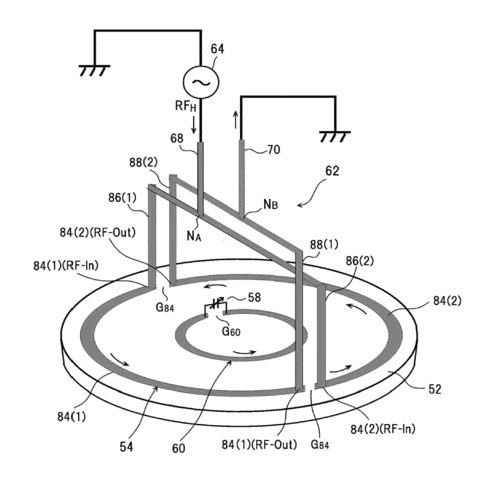
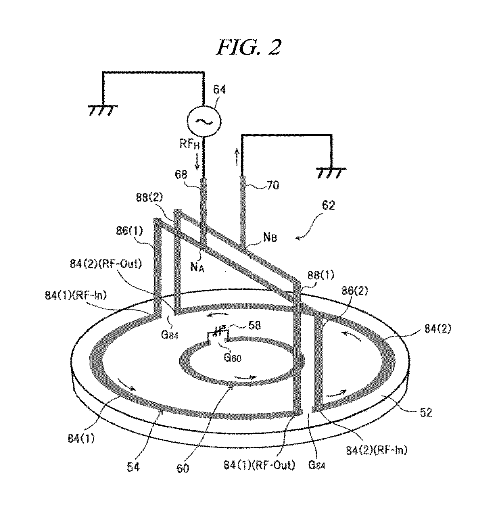
In an inductively coupled plasma processing apparatus, it is possible to control a plasma density distribution while suppressing a wavelength effect within a RF antenna. Provided at a ceiling of a chamber 10 or above a dielectric window 52 is a circular ring-shaped RF antenna 54 for generating inductively coupled plasma within the chamber 10. This RF antenna 54 includes two coil segments 84(1) and 84(2) each having a semicircular arc shape. The coil segments 84(1) and 84(2) are electrically connected to each other in parallel with respect to a high frequency power supply unit 62. On the dielectric window 52, a circular ring-shaped floating coil 60 having a variable capacitor 58 coupled to the RF antenna 54 by an electromagnetic induction is provided. The variable capacitor 58 is varied in a certain range by a capacitance varying unit 82 under the control of a main controller 80.

Description

CROSS-REFERENCE TO RELATED APPLICATION[0001]This application claims the benefit of Japanese Patent Application No. 2011-074875 filed on Mar. 30, 2011, and U.S. Provisional Application Ser. No. 61 / 472,654 filed on Apr. 7, 2011, the entire disclosures of which are incorporated herein by reference.FIELD OF THE INVENTION[0002]The present disclosure relates to a technique for performing a plasma process on a processing target substrate; and, more particularly, to an inductively coupled plasma processing apparatus.BACKGROUND OF THE INVENTION[0003]In a manufacturing process of a semiconductor device or a FPD (Flat Panel Display), plasma is used to perform a process, such as etching, deposition, oxidation or sputtering, so as to perform a good reaction of a processing gas at a relatively low temperature. Conventionally, plasma generated by a high frequency electric discharge in MHz frequency band has been used in this kind of plasma process. The plasma generated by the high frequency electr...

Claims


Application Information

Patent Timeline
Patent Type & Authority Patents(United States)
IPC IPC(8): H01L21/306C23C16/00H01J37/32
CPCH01J37/321H01J37/3211
Inventor YAMAZAWA, YOHEI
Owner TOKYO ELECTRON LTD
Learn More