Method of dicing thin semiconductor substrates

a technology of semiconductor substrates and dicing methods, which is applied in the direction of manufacturing tools, welding/soldering/cutting articles, laser beam welding apparatus, etc., can solve the problems of increasing the difficulty of cutting thin semiconductor substrates, cracks and/or breakage of singulated semiconductor dice, and unattractive mass production process, so as to preserve the strength of integrated devices and reduce structural damage to the sides.

Active Publication Date: 2016-04-12
ASMPT SINGAPORE PTE LTD
View PDF4 Cites 8 Cited by
  • Summary
  • Abstract
  • Description
  • Claims
  • Application Information

AI Technical Summary

Benefits of technology

[0006]It is thus an object of the invention to seek to provide a method of dicing thin semiconductor substrates that reduces structural damage to the sides of singulated integrated devices as compared to conventional laser dicing processes, so as to preserve the die strengths of the integrated devices that are singulated thereby.

Problems solved by technology

As such semiconductor substrates become thinner for the production of thin semiconductor dice used in ever-smaller end-products, it has become increasingly challenging to cut thin semiconductor substrates, which are now manufactured in the order of 100 μm thickness or less.
However, it has been found that applying mechanical force with the saw blade leads to cracks in and / or breakage of the singulated semiconductor dice.
This makes it an unattractive process for mass production.
On the other hand, the two-step dice-before-grind approach is slow and is also not ideal for mass production.
This results in ablation of the material of the semiconductor substrate through melting and evaporation, until the integrated devices are separated.
A negative side-effect of such high laser intensity is that the heat damages the sides of the singulated integrated device.
This heat damage results in significant reduction of die strength in the integrated devices, which is particularly problematic in the case of thin semiconductor substrates.
While the die strength could in principle be recovered at least in part in a post-process etching step, the etching process requires aggressive chemicals that might damage active components on the semiconductor die, as well as the carrier (usually an adhesive tape) on which the semiconductor substrate is mounted.

Method used


Image

  • Method of dicing thin semiconductor substrates
  • Method of dicing thin semiconductor substrates
  • Method of dicing thin semiconductor substrates

Examples


Embodiment Construction

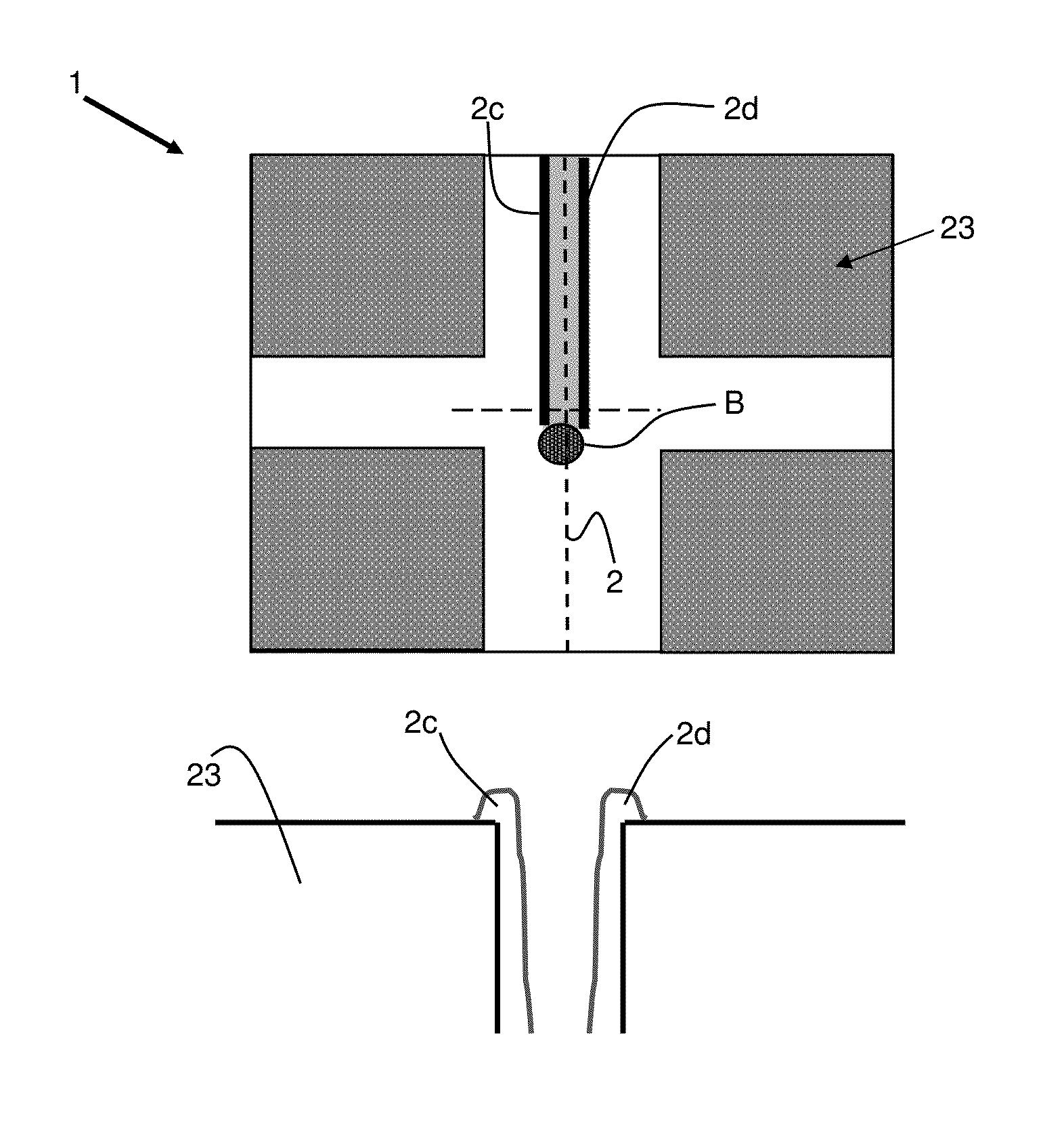
[0015]FIG. 1 is a front elevation view of part of a laser dicing apparatus that is applicable for implementing the current invention. The laser dicing apparatus is operable to radiatively dice a substantially planar semiconductor substrate 1 along at least one cutting line on a target surface 3 of the substrate 1 using laser energy.

[0016]Specifically, FIG. 1 shows a substrate holder H, which may be in the form of a table or chuck, for supporting the substrate 1 during dicing. An illuminator I is located above the substrate holder H for producing a laser beam output B which may comprise one or more laser beams. A projection system P is located underneath the illuminator I for focusing the laser beam output B onto the target surface 3 of the substrate 1 when it is supported on the substrate holder H. The region of impingement of the laser beam output B upon the substrate 1 is denoted by T. Further, an actuator system A such as a stage assembly causes relative displacement of the subst...


PUM

PropertyMeasurementUnit
thicknessaaaaaaaaaa
anglesaaaaaaaaaa
transverse distanceaaaaaaaaaa

Abstract

A method of dicing a plurality of integrated devices included in a semiconductor substrate using laser energy comprises the steps of directing a first laser beam onto a cutting line along the substrate to ablate a portion of the substrate located along the cutting line to be diced, the portion of the substrate that is ablated forming a recast material adjacent to the cutting line of the substrate that has been diced. A second laser beam is directed onto another portion of the substrate adjacent to the cutting line to conduct heat processing of the recast material formed adjacent to the cutting line.

Description

FIELD OF THE INVENTION[0001]The invention relates to the cutting or dicing of semiconductor substrates typically in the form of semiconductor wafers, and in particular, to the dicing of thin semiconductor substrates.BACKGROUND AND PRIOR ART[0002]Semiconductor substrates in the form of wafers are diced to form singulated integrated devices or chips. As such semiconductor substrates become thinner for the production of thin semiconductor dice used in ever-smaller end-products, it has become increasingly challenging to cut thin semiconductor substrates, which are now manufactured in the order of 100 μm thickness or less.[0003]Thin semiconductor substrates can be diced using a mechanical blade saw or by partially dicing a thicker semiconductor substrate with a mechanical blade saw, and then grinding the semiconductor substrate until the semiconductor dice are separated. However, it has been found that applying mechanical force with the saw blade leads to cracks in and / or breakage of the...

Claims


Application Information

Patent Timeline
Patent Type & Authority Patents(United States)
IPC IPC(8): B23K26/00H01L21/00B29C35/08H01L21/268H01L21/78B23K26/073B23K26/36
CPCH01L21/78H01L21/268B23K26/073B23K26/362B23K2201/40B23K26/0604B23K26/38B23K26/0608B23K26/40B23K26/364B23K2103/56
Inventor VAN DER STAM, KAREL MAYKEL RICHARDKNIPPELS, GUIDO MARTINUS HENRICUSMUELLER, MARK CHRISTIANBETZ, JUERGEN ROLAND
Owner ASMPT SINGAPORE PTE LTD
Why Eureka
Try Eureka