Method of laser lift-off for light-emitting diode

A technology of light-emitting diodes and laser stripping, applied in laser welding equipment, electrical components, circuits, etc., can solve problems such as damage to the adhesive metal layer, and achieve the effect of reducing stress damage to the structure

Inactive Publication Date: 2011-05-11
HIGH POWER OPTO
View PDF2 Cites 3 Cited by
  • Summary
  • Abstract
  • Description
  • Claims
  • Application Information

AI Technical Summary

Problems solved by technology

[0011] Therefore, the main purpose of the present invention is to solve the problem of twice irradiating the bonded metal layer in the isolation channel, solve the problem that the bonded metal layer is heated twice, so that the structure of the bonded metal layer is destroyed, and improve the yield of the crystal grain

Method used


Image

  • Method of laser lift-off for light-emitting diode
  • Method of laser lift-off for light-emitting diode
  • Method of laser lift-off for light-emitting diode

Examples


Embodiment Construction

[0026] Therefore, the details and technical descriptions of the present invention will be further described through examples, but it should be understood that these examples are only examples and should not be construed as limitations on the implementation of the present invention.

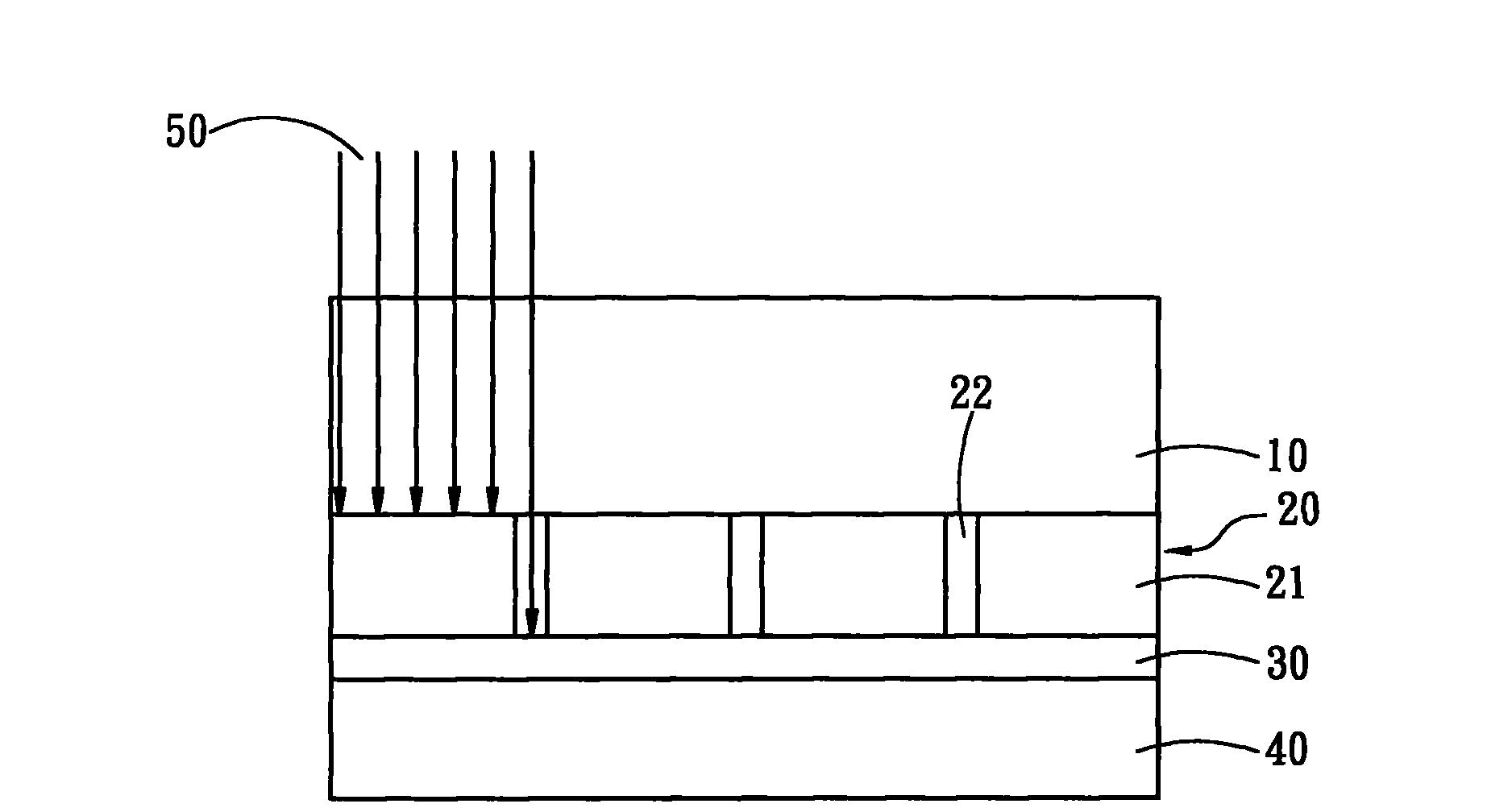
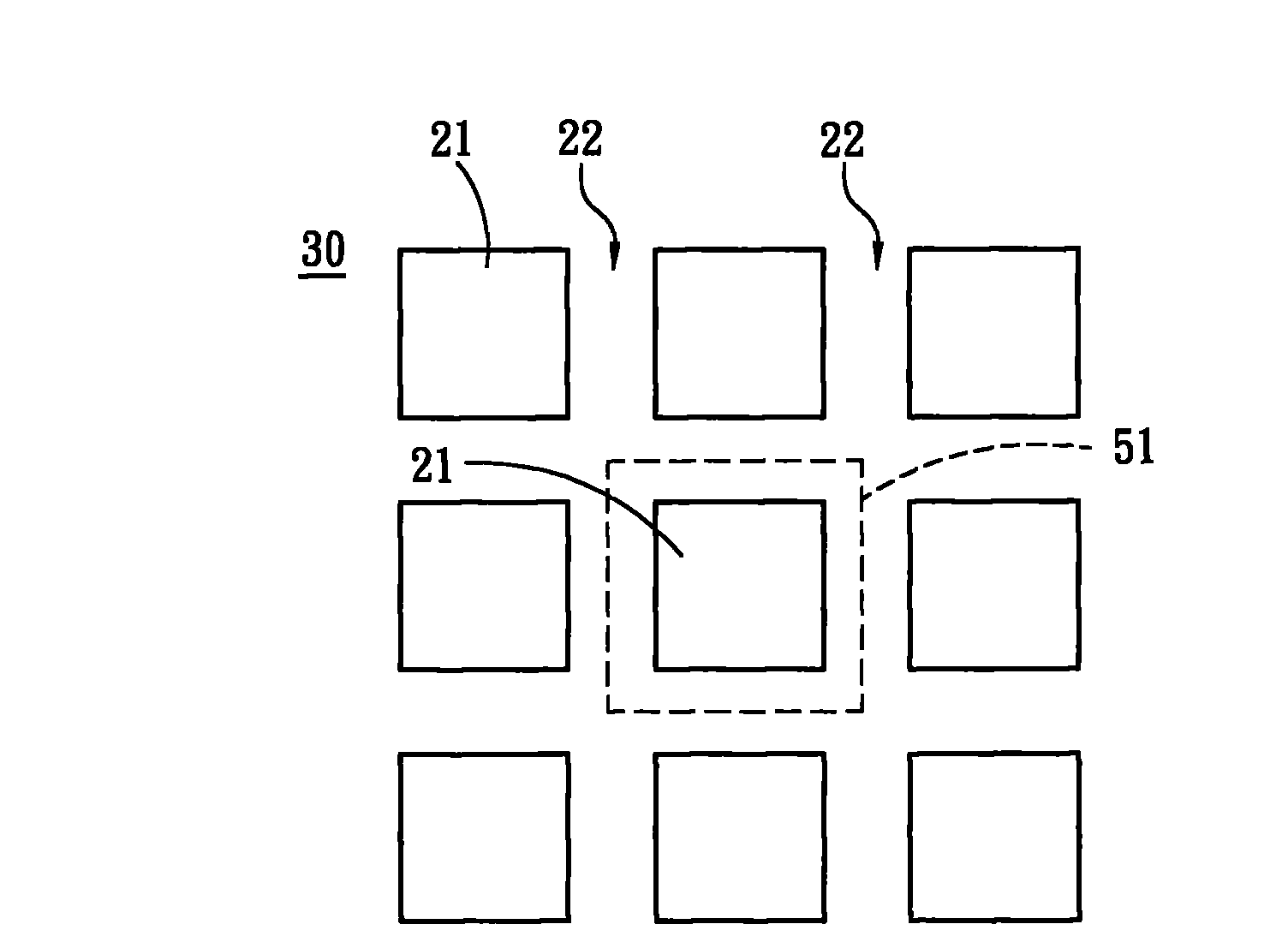
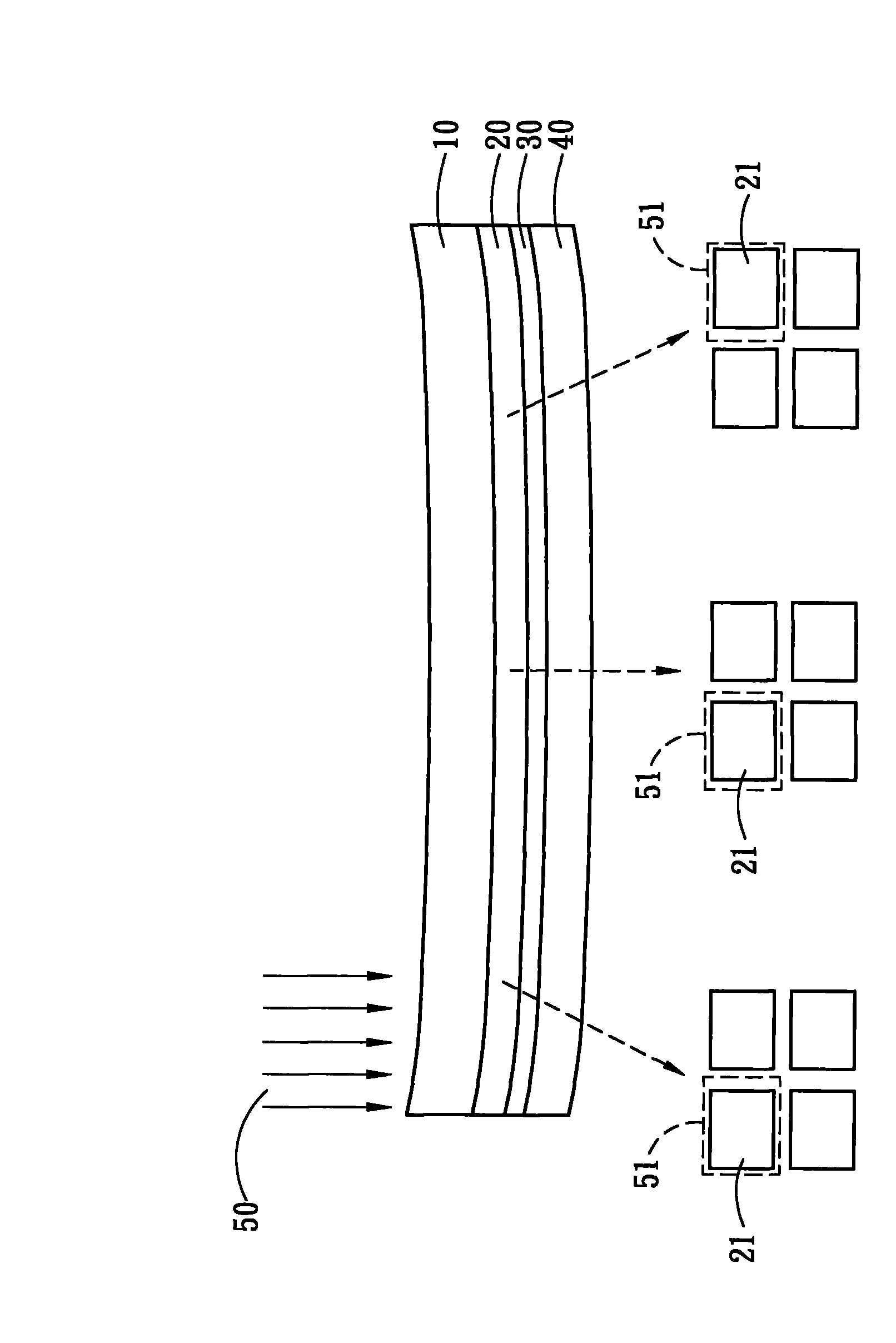
[0027] refer to Figure 5 , The present invention is applied to the existing method of laser lift-off of light-emitting diodes. In the implementation of the method of laser lift-off of light-emitting diodes, an epitaxial layer 200 for light emission is sequentially formed on a conversion substrate 100 (such as a sapphire substrate). Different from the known method of laser lift-off of light-emitting diodes, the present invention etches the epitaxial layer 200 to define an isolation road 220 around each grain region 210, and between two adjacent isolation roads 220 there is an undisturbed An isolation region 230 of the material of the epitaxial layer 200 is etched. Therefore, the pitch of the die ...


PUM

PropertyMeasurementUnit
widthaaaaaaaaaa
widthaaaaaaaaaa

Abstract

The invention relates to a method of laser lift-off for a light-emitting diode. Isolation channels are etched on the periphery of each grain area on an epitaxial layer after the epitaxial layer is formed on a conversion substrate and before a support substrate provided with a bonding metal layer is combined with the epitaxial layer, and a non-etched isolation area is arranged between two adjacentisolation channels. Only the isolation channels and the isolation areas on the periphery of the grain area are irradiated by each laser irradiation through the isolation areas and the bonding metal layer on the isolation channels is heated only once. Stress damage generated by the laser irradiation to the grain area is lightened because an outward stress generated by the isolation area and the outward stress generated by the irradiated grain areas cancel each other.

Description

technical field [0001] The invention relates to a method for laser lift-off of light-emitting diodes, in particular to a method for laser lift-off of light-emitting diodes used for manufacturing epitaxial layer structures of light-emitting diode grains. Background technique [0002] A main component of a light emitting diode (Light Emitting Diode, LED) is an LED grain, which is formed by multiple epitaxy of a light-emitting semiconductor material. LED grains are mainly composed of semiconductor materials such as gallium phosphide (GaP), gallium aluminum arsenide (GaAlAs), or gallium arsenide (GaAs), gallium nitride (GaN) and other semiconductor materials, and its internal structure is a PN junction with unidirectional Electricity. [0003] Taking the blue light-emitting diode as an example, it is generally made of sapphire (Al 2 o 3 ) substrate for growing higher-quality gallium nitride-based (GaN-based) epitaxial thin films. However, the poor electrical and thermal cond...

Claims


Application Information

Patent Timeline
Patent Type & Authority Applications(China)
IPC IPC(8): H01L21/78H01L21/268B23K26/40H01L33/00
Inventor 颜良吉李逸骏
Owner HIGH POWER OPTO
Why Eureka
Try Eureka