

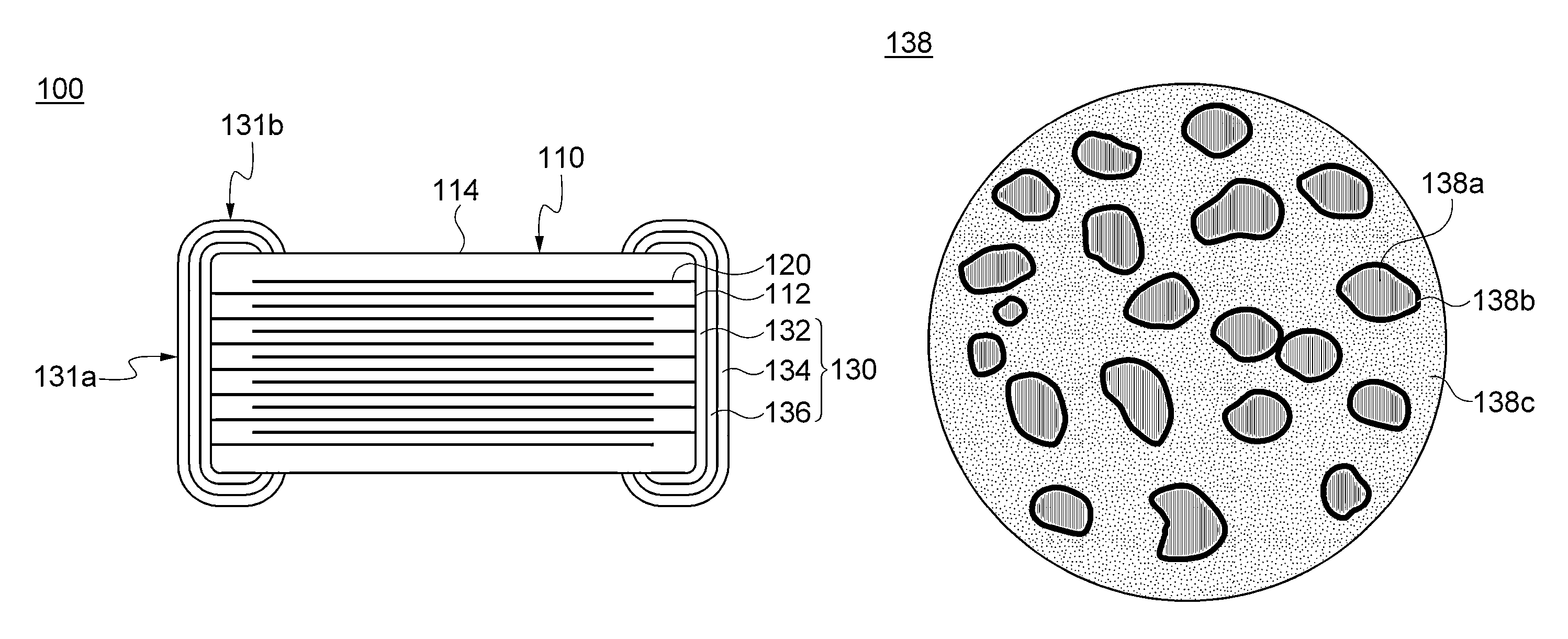
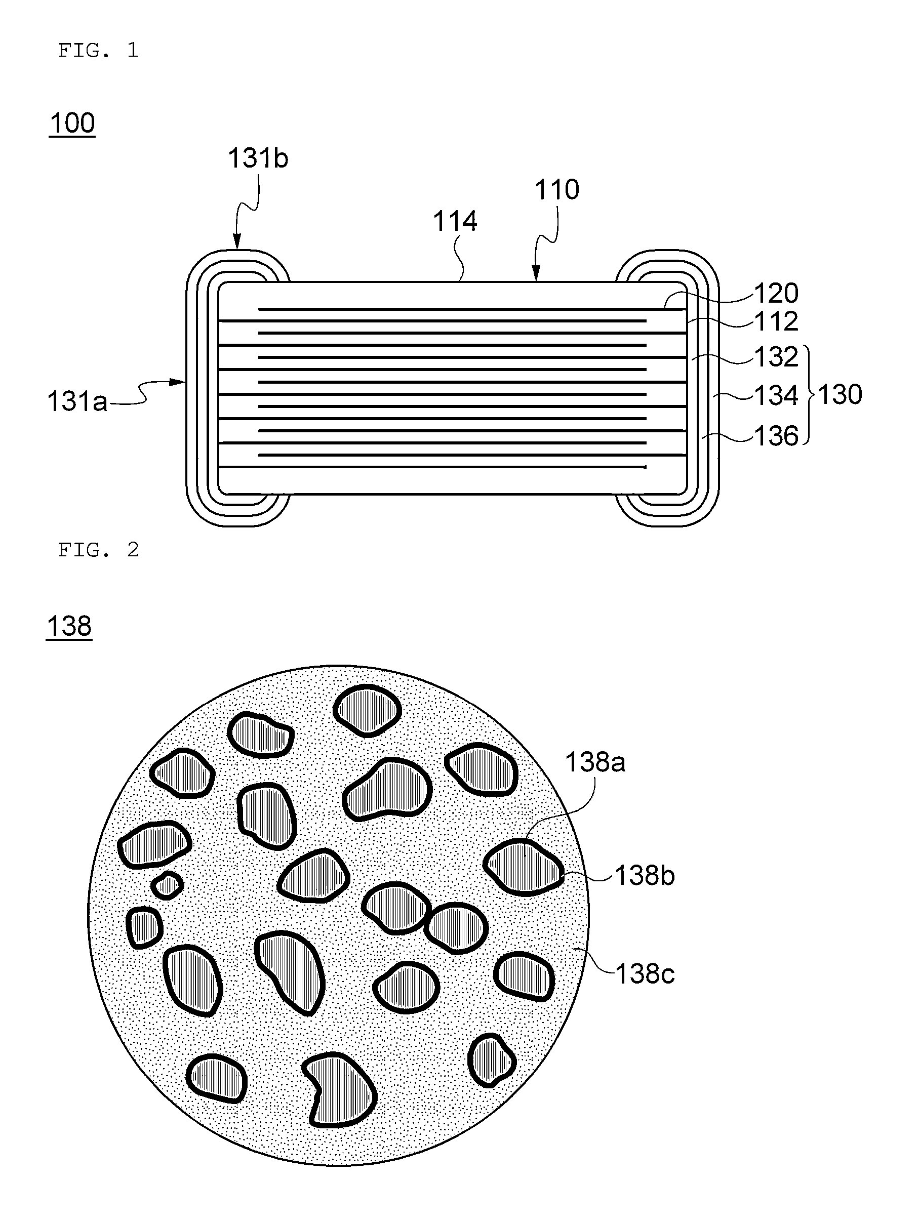
Multilayer ceramic device
a ceramic device and multi-layer technology, applied in the direction of fixed capacitor details, stacked capacitors, fixed capacitors, etc., can solve the problems of thermal impact, cracks on the surface of the device body, relative vulnerability to physical pressure or impact,
- Summary
- Abstract
- Description
- Claims
- Application Information
AI Technical Summary
Benefits of technology
Problems solved by technology
Method used
Image

Examples
example
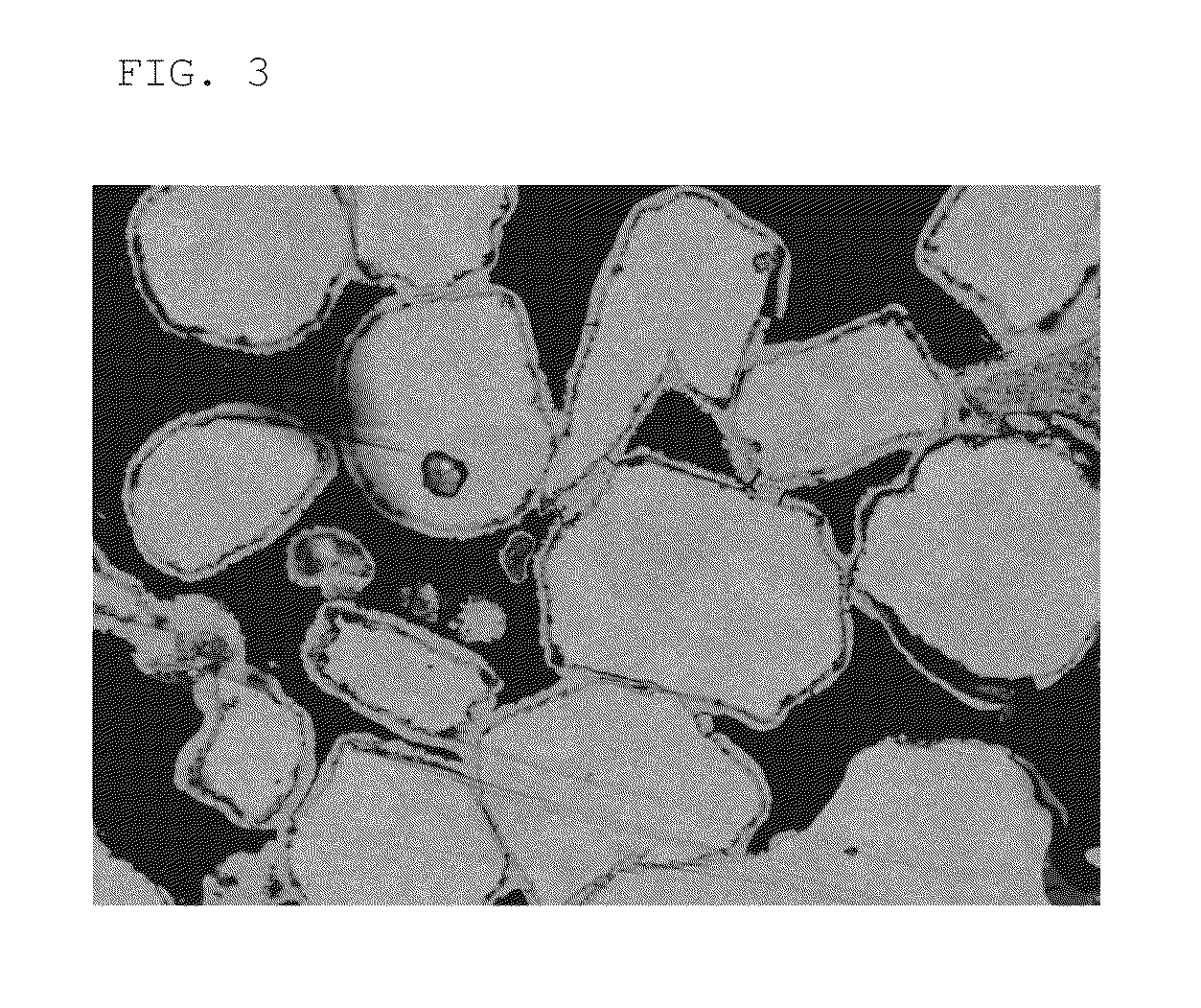
[0041]500 multilayer ceramic devices with the size 1.6 mm×0.8 mm×0.8 mm of and the capacitance of 1 nF were manufactured. Here, the external electrode of the multilayer ceramic device is separately manufacture as a normal structure (with an electrode in Cu layer only) and as a soft electrode structure (with an intermediate layer as well as the electrode in Cu layer). In the case of the manufactured soft electrode structure, in order to evaluate the effects on the metal oxide film, the curing process for curing the external electrode among the manufacturing process of the multilayer ceramic device, was performed under different atmosphere conditions, in order to manufacture a number of samples. Here, as indicated in Table 1, the curing atmosphere was controlled by adjusting a flux rate between nitrogen gas (N2) and air. In addition, the thickness of the metal oxide film in the intermediate layer of the resulting samples was measured by scanning electron microscopy (SEM).
[0042]For fle...
PUM
| Property | Measurement | Unit |
|---|---|---|
| thickness | aaaaa | aaaaa |
| thickness | aaaaa | aaaaa |
| capacitance | aaaaa | aaaaa |
Abstract
Description
Claims
Application Information