

Gallium nitride materials including thermally conductive regions
a technology of gallium nitride and thermal conductivity, which is applied in the direction of semiconductor devices, electrical equipment, and semiconductor/solid-state device details, etc., can solve the problems of poor thermal conductivity, large localized heat generation in active device areas and/or highly resistive regions, and performance problems, so as to achieve effective distribution and/or dissipation of heat in gallium nitride material devices, poor thermal conductivity, and poor thermal conductivity
- Summary
- Abstract
- Description
- Claims
- Application Information
AI Technical Summary
Benefits of technology
Problems solved by technology
Method used
Image

Examples
Embodiment Construction
[0028] The invention provides gallium nitride material devices including thermally conductive regions and methods to form such devices.
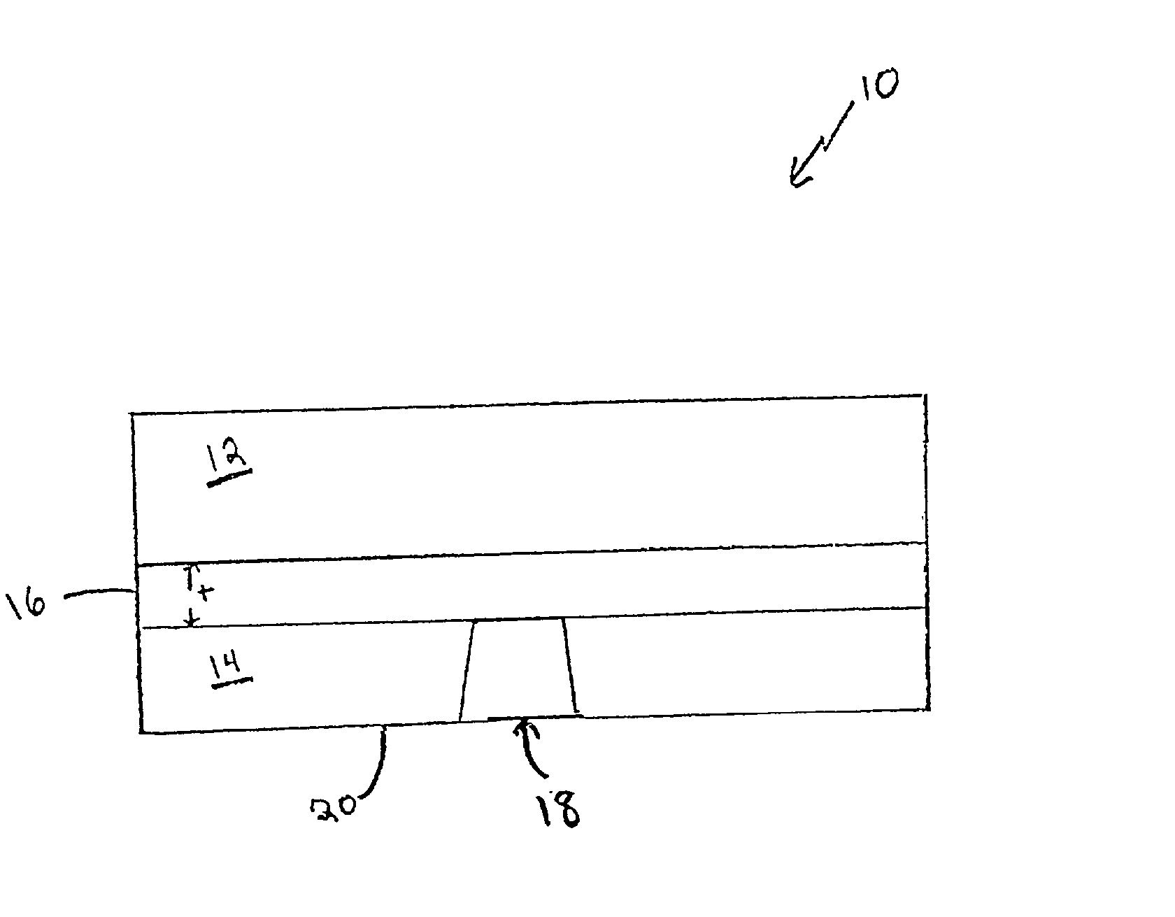
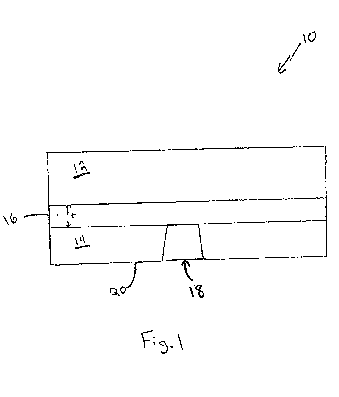
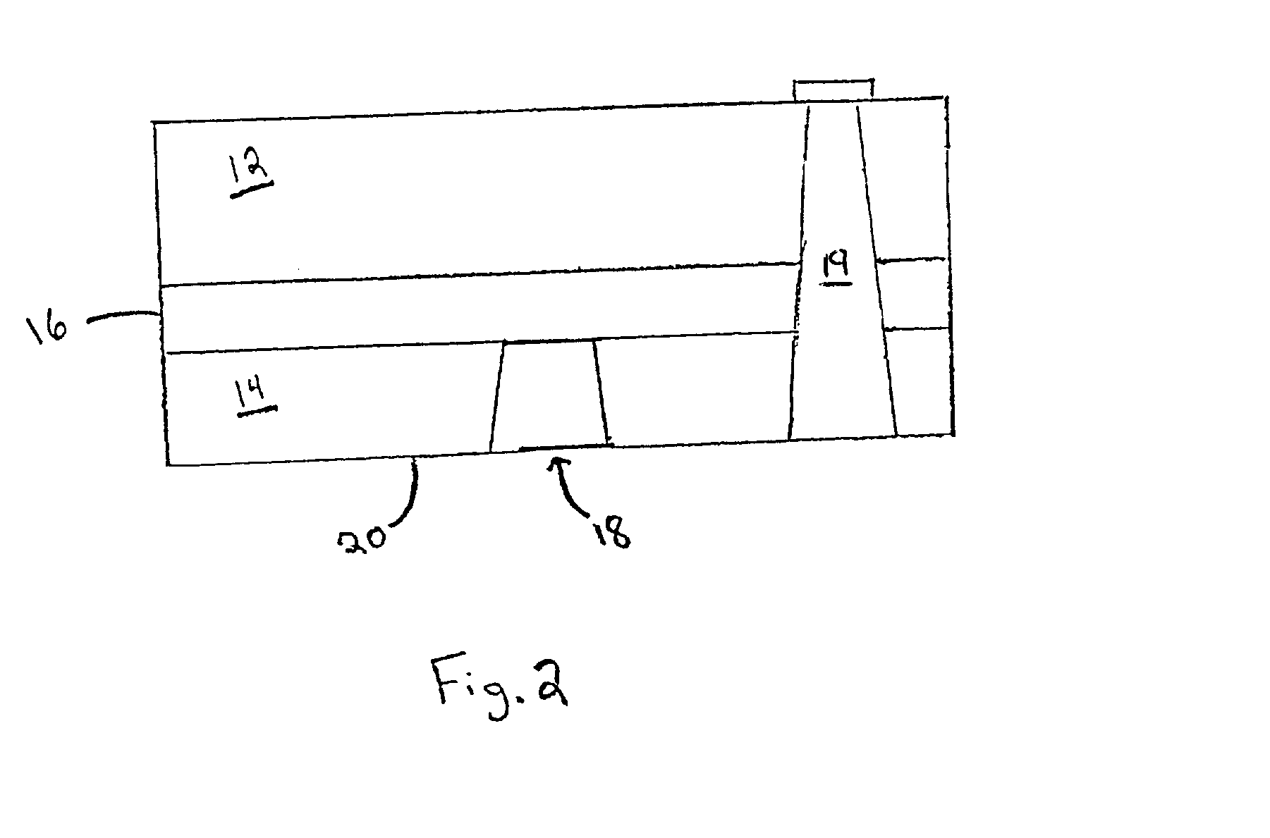
[0029] Referring to FIG. 1, a semiconductor device 10 according to one embodiment of the invention is shown. Device 10 includes a gallium nitride material device region 12 formed over a substrate 14. As described further below, device structures are typically formed, at least in part, within gallium nitride material device region 12. A heat spreading layer 16 is formed between gallium nitride material region 12 and substrate 14. Heat spreading layer 16 distributes heat generated within device region 12 which otherwise may damage the device or effect performance. In the illustrative embodiment, device 10 also includes a heat sink 18 that extends from a backside 20 of the device. As shown, heat sink 18 is connected to spreading layer 16 so that heat conducted from the spreading layer may be dissipated, for example to the environment, by the heat sink.
[...
PUM
| Property | Measurement | Unit |
|---|---|---|
| thickness | aaaaa | aaaaa |
| thickness | aaaaa | aaaaa |
| thickness | aaaaa | aaaaa |
Abstract
Description
Claims
Application Information