Integrated thermoelectric cooling devices and methods for fabricating same

a technology of thermoelectric cooling devices and thermoelectric components, applied in the manufacture/treatment of thermoelectric devices, semiconductor devices, semiconductor/solid-state device details, etc., can solve the problems of increasing system performance limitations, increasing power density, and increasing efficiency, and achieve rapid and precise temperature control through local heating or cooling operations. , the effect of increasing heat removal

Active Publication Date: 2006-05-18
GLOBALFOUNDRIES US INC
View PDF10 Cites 121 Cited by
  • Summary
  • Abstract
  • Description
  • Claims
  • Application Information

AI Technical Summary

Benefits of technology

[0010] In general, exemplary embodiments of the invention include semiconductor integrated thermoelectric cooling devices comprising high-density arrays of thermoelectric elements, which are fabricated using semiconductor thin-film and VLSI (very large scale integration) processes. Exemplary methods for constructing thermoelectric devices according to the invention enable a significant reduction of the dimensions of TE elements using advanced thin-film material and technologies to provide a significant improvement in heat pumping capacity of the integrated TE devices as compared to conventional modules. For instance, ultra high-density TE devices according to embodiments of the invention may be formed to include 20 million cells per centimeter square and 50 I / Os, yielding a heat removing capacity of 1200 W / cm2.

Problems solved by technology

Effective heat removal becomes increasingly problematic as chip geometries are scaled down and circuit devices and chips are more densely packed, and operating speeds are increased, which result in increased power density.
Indeed, increased system performance is limited primarily by the ability to implement effective heat removal mechanisms to cool the IC chip modules.
Although conventional thermoelectric devices such as described with reference to FIG. 1 may be implemented for cooling IC chips, such devices comprise very low-density TE element arrays and, consequently, do not provide the required cooling capacity for cooling high-performance chips or package structures with high-power densities.

Method used


Image

  • Integrated thermoelectric cooling devices and methods for fabricating same
  • Integrated thermoelectric cooling devices and methods for fabricating same
  • Integrated thermoelectric cooling devices and methods for fabricating same

Examples


Embodiment Construction

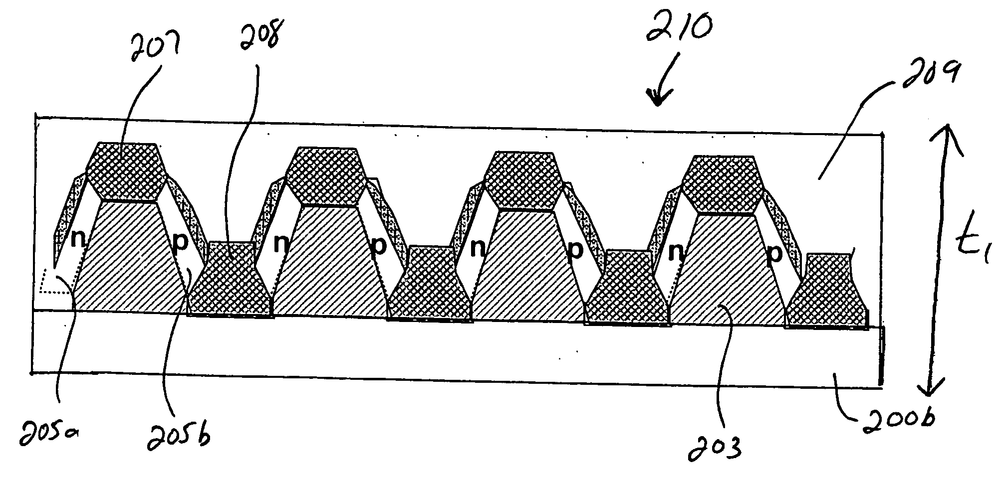
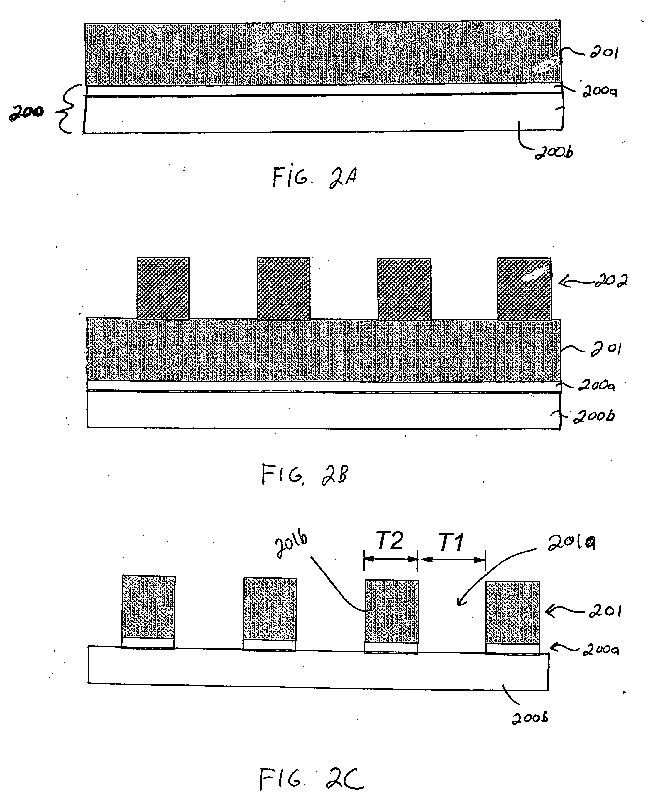
[0026] FIGS. 2A˜2K illustrate a method for fabricating a high-density semiconductor integrated thermoelectric cooling device according to an exemplary embodiment of the present invention. More specifically, FIGS. 2A˜2K illustrate a method for fabricating a high-density thermoelectric cooling module using semiconductor thin-film and VLSI (very large scale integration) processes. Referring to FIG. 2A, an initial step includes forming a first insulating film layer (201) (e.g., dielectric film) on a semiconductor substrate (200). The semiconductor substrate (200) comprises a layer of silicon (200a) formed on a buried oxide layer (200b). Depending on the application, the substrate (200) may comprise a SOI (silicon-on-insulator) substrate. In an exemplary embodiment wherein the substrate (200) is an SOI substrate, the back (bottom) of the substrate (200) would comprise a thick bulk silicon layer (not shown) with the buried oxide layer (200b) interposed between the bulk silicon layer and t...


PUM


Abstract

Semiconductor integrated thermoelectric devices are provided, which are formed having high-density arrays of thermoelectric (TE) elements using semiconductor thin-film and VLSI (very large scale integration) fabrication processes. Thermoelectric devices can be either separately formed and bonded to semiconductor chips, or integrally formed within the non-active surface of semiconductor chips, for example.

Description

TECHNICAL FIELD OF THE INVENTION [0001] The present invention relates generally to devices and methods for cooling electronic devices such as semiconductor integrated circuit (IC) chips. More particularly, the invention relates to devices and methods for constructing semiconductor integrated thermoelectric cooling modules having high-density arrays of thermoelectric (TE) elements using semiconductor thin-film and VLSI (very large scale integration) fabrication processes. BACKGROUND [0002] In general, thermoelectric cooling devices are solid state heat pumps that are used in a variety of applications where thermal management is required. For instance, thermoelectric cooling modules are implemented for actively cooling electronic components such as semiconductor IC (integrated circuit) chips. By way of example, FIG. 1 schematically illustrates a conventional apparatus (100) for cooling an electronic device. In general, the apparatus (100) comprises a thermoelectric (TE) module (101) t...

Claims


Application Information

Patent Timeline
Patent Type & Authority Applications(United States)
IPC IPC(8): H01L35/34H01L35/30H01L37/00
CPCH01L23/38H01L27/16H01L35/32H01L35/34H01L2224/16225H01L2924/00014H01L2924/00011H10N19/00H10N10/01H10N10/17H01L2224/0401
Inventor CHEN, HOWARD HAOCHU, RICHARD C.HSU, LOUIS L.
Owner GLOBALFOUNDRIES US INC
Why Eureka
Try Eureka