Slot designs in wide metal lines

a technology of metal lines and slots, applied in the direction of semiconductor devices, semiconductor/solid-state device details, electrical devices, etc., can solve the problems of opportunistic assumption, and achieve the effect of relieving stress-induced voids and vacancies

Active Publication Date: 2016-04-19
CHARTERED SEMICONDUCTOR MANUFACTURING +1
View PDF74 Cites 0 Cited by
  • Summary
  • Abstract
  • Description
  • Claims
  • Application Information

AI Technical Summary

Benefits of technology

[0012]Embodiments of the present invention provides a structure and method of forming an interconnect structure comprising a wide line having a slot. The slot relieves stress induced voids and vacancies in the interconnect.
[0013]An embodiment is an interconnect structure with slot(s) in wide lines to reduce stress. The interconnect structure preferably comprises: an interconnect comprising a wide line; the wide line has a first slot; a via plug in contact with the wide line from above or below; the first slot is spaced a first distance from a via plug so that the first slot relieves stress and / or induced voiding on the wide line and the via plug.
[0014]Another embodiment is a dual damascene interconnect Structure comprising: an dual damascene shaped interconnect comprising a via plug, a first slot and a wide line; said wide line having said first slot; said first slot is spaced a first distance from said via plug so that said first slot relieves stress on the wide line and the via plug.
[0015]Another embodiment is an interconnect structure comprising: a lower interconnect comprised of a wide line; said wide line having a first slot; an upper interconnect comprised of a via plug; said via plug contacting the top surface of said wide line; said first slot is spaced a first distance from said via plug so that said first slot relieves stress on the wide line and the via plug.

Problems solved by technology

However, this assumption has been illustrated to be opportunistic because of copper's strong dependency on process and structure.

Method used


Image

  • Slot designs in wide metal lines
  • Slot designs in wide metal lines
  • Slot designs in wide metal lines

Examples


Embodiment Construction

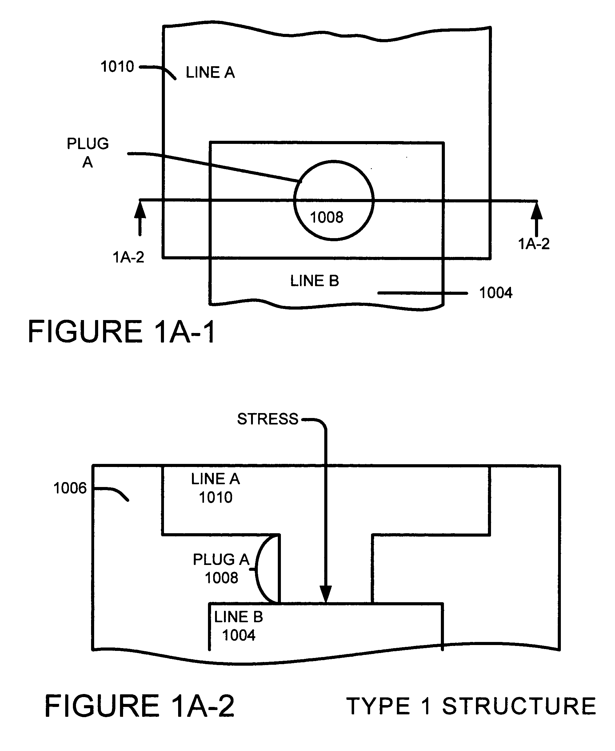
[0028]Referring now to the drawings and more particularly to FIG. 1A-1 and FIG. 1A-2, there is shown an example structure over which example embodiments of the present invention are an improvement. It is to be understood in this regard that no portion of FIG. 1A-1 or FIG. 1A-2 are admitted to be prior art. Rather, this highly simplified diagram is an effort to provide an improved understanding of some problems.

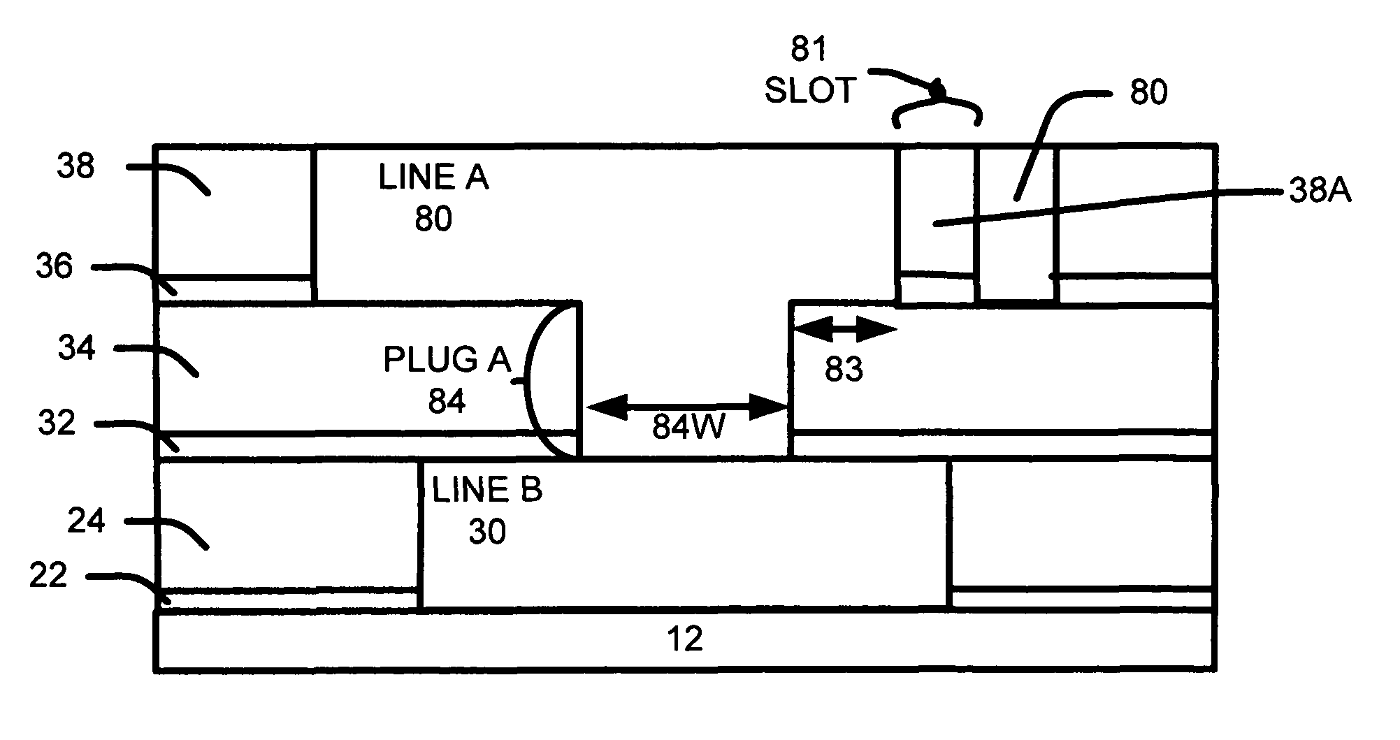
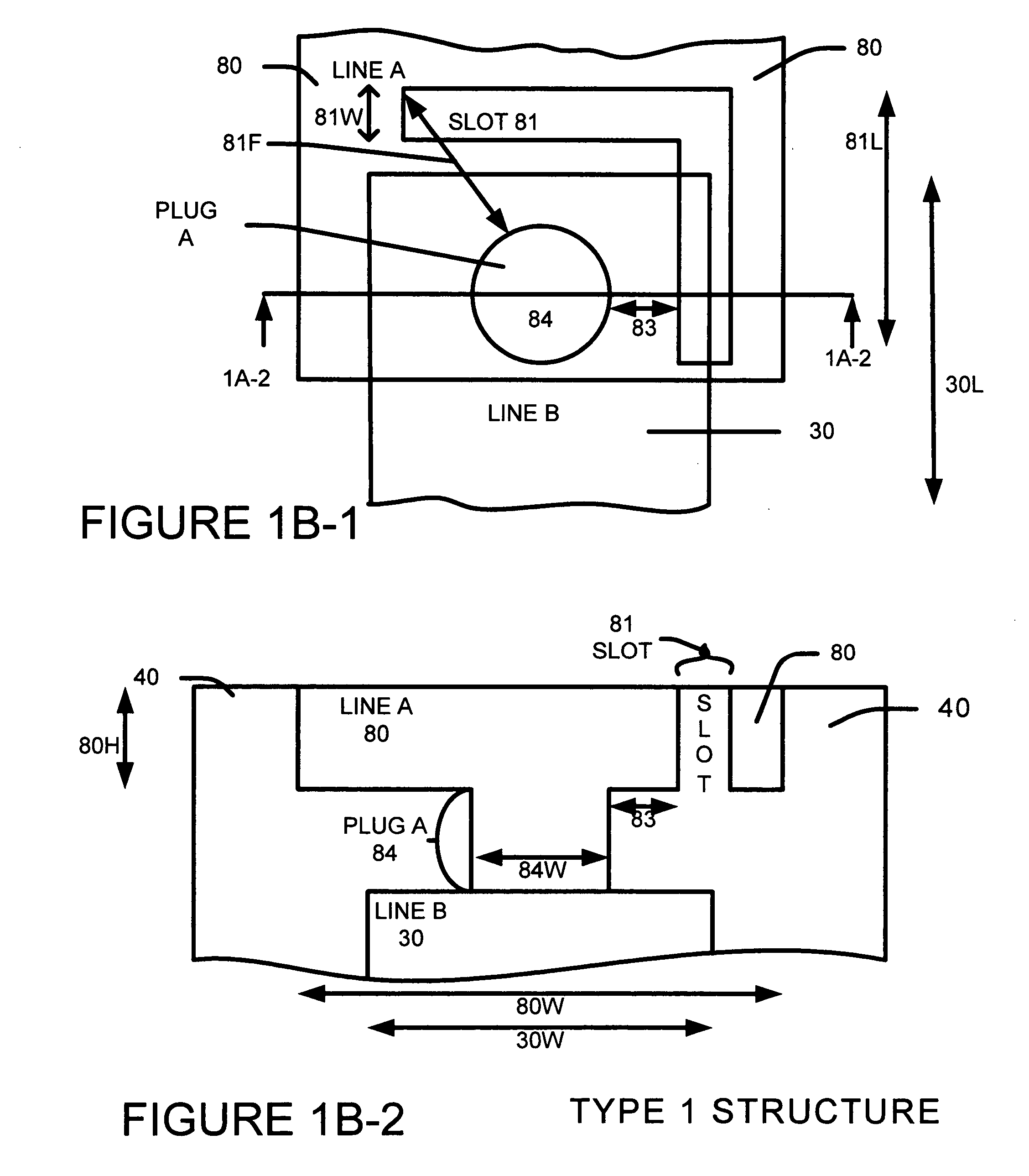
Type 1 Stress—Wide Line 1010 Over the Via Plug 1008 that Contacts the Lower Line 1004

[0029]FIG. 1A-1 shows a top down view of the upper dual damascene interconnect 10081010, an underlying line 1004 and a dielectric 1006. FIG. 1A-2 shows a cross sectional view. The upper dual damascene interconnect is comprised of a via plug 1008 and a wide line 1010. Type 1 stress 1014 is created by the wide line 1010 over the via plug 1008 that contacts the lower line (interconnect) 1004.

[0030]Type 1 Stress induced voiding mechanisms can include: 1) vacancies / void migration to via bottom and ...


PUM


Abstract

A method and structure for slots in wide lines to reduce stress. An example embodiment method and structure for is an interconnect structure comprising: interconnect comprising a wide line. The wide line has a first slot. The first slot is spaced a first distance from a via plug so that the first slot relieves stress on the wide line and the via plug. The via plug can contact the wide line from above or below. Another example embodiment is a dual damascene interconnect structure comprising: an dual damascene shaped interconnect comprising a via plug, a first slot and a wide line. The wide line has the first slot. The first slot is spaced a first distance from the via plug so that the first slot relieves stress on the wide line and the via plug.

Description

BACKGROUND OF INVENTION[0001]1) Field of the Invention[0002]This invention relates generally to design and fabrication of metal lines and more particularly to fabrication of slots in metal lines for semiconductor devices.[0003]2) Description of the Prior Art[0004]The downward scaling of feature sizes in very large scale integration (VLSI) fabrication has resulted in the transition of the interconnect technology from Aluminum (Al) to Copper (Cu) for faster device performance. Owing to the differences between Al and Cu process, studies on the reliability performance such as electromigration (EM) between Al and Cu interconnects had since rose in importance. Less attention has been focused on the study of stress-induced voiding in Cu interconnects because of its favorable properties such as lower mobility and similar intrinsic stress level as compared to Al interconnects. However, this assumption has been illustrated to be opportunistic because of copper's strong dependency on process a...

Claims


Application Information

Patent Timeline
Patent Type & Authority Patents(United States)
IPC IPC(8): H01L21/76H01L21/768H01L23/522H01L23/528H01L23/532
CPCH01L21/76816H01L21/76802H01L21/76808H01L23/528H01L23/5226H01L23/53295H01L2924/0002H01L2924/00H01L21/0276H01L21/288H01L21/3212H01L21/7684H01L21/76843H01L21/7685H01L21/76879H01L23/53228H01L23/562
Inventor LIM, YEOW KHENGSEE, ALEXLEE, TAE JONGVIGAR, DAVIDHSIA, LIANG CHOOPEY, KIN LEONG
Owner CHARTERED SEMICONDUCTOR MANUFACTURING
Why Eureka
Try Eureka