
Electroless plating method using halide

a technology of halide and electroless plating, which is applied in the field of electroless plating methods, can solve the problems of affecting the physical health of the human body or neighboring devices or instruments, the use of ito coatings, and the inability to meet the requirements of the application of the metal, so as to promote polymer crosslinking, increase the hydrophilicity of exposed regions, and promote strong adhesion of the polymeric layer

Active Publication Date: 2016-05-03
EASTMAN KODAK CO
View PDF12 Cites 0 Cited by
  • Summary
  • Abstract
  • Description
  • Claims
  • Application Information

AI Technical Summary

Benefits of technology

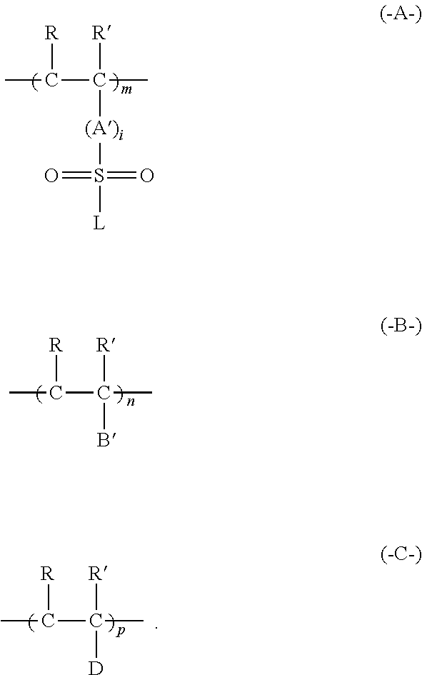
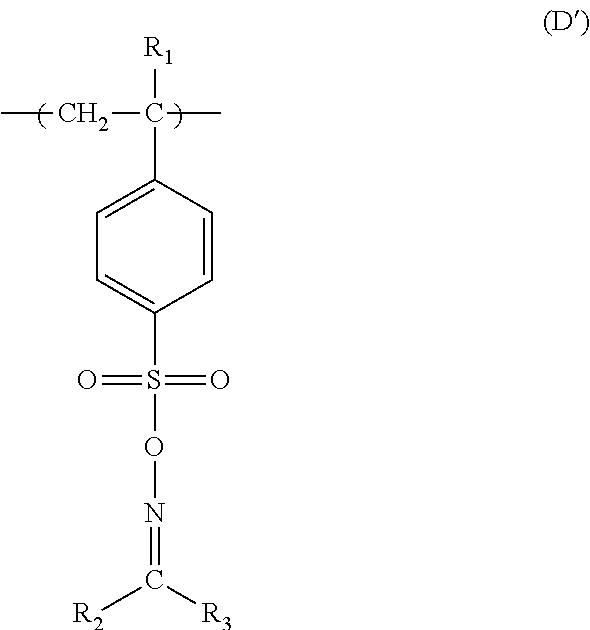
[0032]The present invention provides an efficient method for forming conductive metal patterns using a specifically designed reactive polymer that can be de-blocked and crosslinked for pattern formation. The reactive polymer can undergo one or more chemical reactions upon irradiation to provide pendant sulfonic acid groups and to provide sites that promote polymer crosslinking in the reactive composition as well as reactive sites that will complex with catalytic metal ions such as silver ions or palladium ions. The chemical reactions also increase the hydrophilicity of exposed regions to allow diffusion of hydrophilic compounds such as aqueous metal ions, dyes, non-reducing reagents, and reducing agents and to promote strong adhesion of the polymeric layer to a substrate using crosslinking to minimize dissolution in various aqueous-based baths, solutions, or dispersions used in electroless plating methods.
[0033]The necessary pendant sulfonic acid groups are generated in the reactive polymer during exposure for example to ultraviolet light. The pendant sulfonic acid groups increase the hydrophilicity of the polymer and are available to complex or react with metal ions or other charged molecules.
[0034]The present invention avoids the use of known expensive high vacuum processes necessary for making conductive patterns using indium tin oxide (ITO) coatings and is more readily carried out using high-speed roll-to-roll machines to provide higher manufacturing efficiencies.

Problems solved by technology

As the increase in the use of such devices has exploded in frequency and necessity by displacing older technologies, there has been a concern that electromagnetic radiation emission from such devices may cause harm to the human body or neighboring devices or instruments over time.
Such techniques have a number of disadvantages that are described in this patent and the efforts continue to make additional improvements.
However, the use of ITO coatings has a number of disadvantages.
Indium is an expensive rare earth metal and is available in limited supply.
Moreover, ITO is a ceramic material and is not easily bent or flexed and such coatings require expensive vacuum deposition methods and equipment.
In addition, ITO conductivity is relatively low, requiring short line lengths to achieve desired response rates (upon touch).
These smaller segments require additional driving and sensing electronics, further adding to the cost of the devices.
However, all of these technologies are expensive, tedious, or extremely complicated so that the relevant industries are spending considerable resources to design improved means for forming conductive patterns for various devices especially touch screen displays.

Method used


Image

  • Electroless plating method using halide
  • Electroless plating method using halide
  • Electroless plating method using halide

Examples


##ventive example 1

INVENTIVE EXAMPLE 1

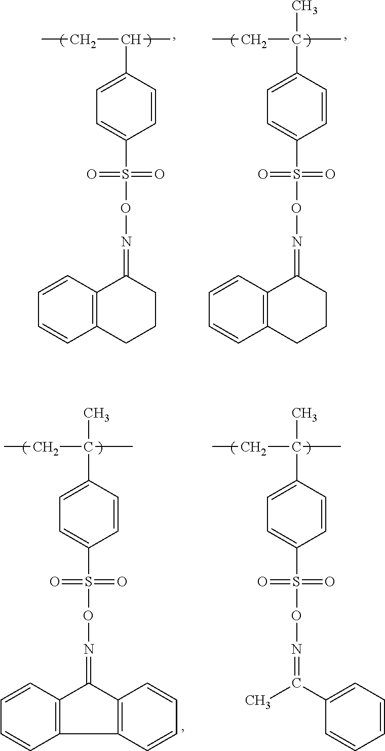
[0227]Polymer A was dissolved in dichloromethane solvent to 15% solids as described above and 3.3 g of this Polymer A solution was added to 1.7 g of cyclopentanone. The resulting reactive composition was spin coated on a PET substrate to form a precursor article. After being dried, the resulting polymeric layer was exposed through a mask to an Oriel high intensity UV lamp for 600 seconds. The exposed polymeric layer was then immersed in a 0.4 molar silver nitrate bath for 3 minutes, rinsed in distilled water for 2 minutes, immersed in a 1 weight % sodium bromide bath for 5 minutes, rinsed in distilled water for 2 minutes, and then dried with compressed nitrogen. The treated polymeric layer was immersed in electroless copper bath C1 for 3 minutes at 20° C., washed in distilled water for 4 minutes, and then dried with compressed nitrogen. The resulting copper pattern exhibited high conductivity in both the large exposed regions and the fine exposed regions (lines) t...

##ventive example 2

INVENTIVE EXAMPLE 2

[0230]Polymer K was dissolved in dichloromethane solvent to 15% solids as per the above method. 3.3 g of this polymer solution was added to 1.7 g cyclopentanone and spin coated onto a PET substrate to form a precursor article. After being dried, the resulting polymeric layer was exposed through a mask to an Oriel high intensity UV lamp for 600 seconds. The exposed polymeric layer was then immersed in a 0.4 molar silver nitrate bath for 3 minutes, rinsed in distilled water for 2 minutes, immersed in a 1 weight % sodium bromide bath for 5 minutes, rinsed in distilled water for 2 minutes, and then dried with compressed nitrogen. The treated polymeric layer was immersed in electroless copper bath Cl for 3 minutes at 20° C., washed in distilled water for 4 minutes, and then dried with compressed nitrogen. The resulting copper pattern exhibited high conductivity in both the large exposed regions and the fine exposed regions (lines) that were 5 to 6 μm in width in the re...

##ventive example 3

INVENTIVE EXAMPLE 3

[0232]Polymer A was dissolved in dichloromethane solvent to 15% solids as described above and 3.3 g of this Polymer A solution was added to 1.7 g of cyclopentanone. The resulting reactive composition was spin coated onto a PET substrate to form a precursor article. After being dried, the resulting polymeric layer was exposed through a mask to an Oriel high intensity UV lamp for 600 seconds. The exposed polymeric layer was then immersed in a 0.4 molar silver nitrate bath for 3 minutes, rinsed in distilled water for 2 minutes, immersed in a 1 weight % sodium bromide bath for 5 minutes, rinsed in distilled water for 2 minutes, and then dried with compressed nitrogen. The treated polymeric layer was uniformly exposed to a hand held 365 nm lamp for 20 minutes, immersed in a 1 weight % dimethylamine borane (DMAB) bath for 5 minutes, rinsed in distilled water for 2 minutes, and dried with compressed nitrogen. The polymeric layer was then immersed in electroless copper ba...


PUM

PropertyMeasurementUnit
widthaaaaaaaaaa
weight %aaaaaaaaaa
energyaaaaaaaaaa

Abstract

A conductive metal pattern is formed using a reactive polymer that can provide pendant sulfonic acid groups upon exposure to radiation, and (2) pendant groups that are capable of providing crosslinking. The polymeric layer is patternwise exposed to radiation to provide first exposed regions that are then contacted with electroless seed metal ions to form a pattern of electroless seed metal ions, followed by contact with a halide. At least some of the electroless seed metal halide can be exposed to form second exposed regions. The polymeric layer can be contacted with a reducing agent either: (i) to develop the electroless seed metal image in the second exposed regions, or (ii) to develop all of the electroless seed metal halide in the first exposed regions, and optionally contacted with a fixing agent. The electroless seed metal nuclei in the first exposed regions can be electrolessly plated with a conductive metal.

Description

RELATED APPLICATIONS[0001]Reference is made to the following related applications:[0002]Copending and commonly assigned U.S. Ser. No. 14 / 084,675 filed on Nov. 20, 2013, by Wexler, Bennett, and Lindner and entitled “Crosslinkable Reactive Polymers.”[0003]Copending and commonly assigned U.S. Ser. No. 14 / 084,693 filed on Nov. 20, 2013, by Irving, Wexler, Bennett, and Lindner and entitled “Forming Conductive Metal Pattern Using Reactive Polymers.”[0004]Copending and commonly assigned U.S. Ser. No. 14 / 084,711 filed on Nov. 20, 2013, by Wexler, Bennett, and Lindner, and entitled “Forming Patterns Using Crosslinkable Reactive Polymers.”[0005]Commonly assigned U.S. Ser. No. 14 / 084,732 filed on Nov. 20, 2013 (now issued as U.S. Pat. No. 9,081,281), by Irving and entitled “Electroless Plating Method.”[0006]Copending and commonly assigned U.S. Ser. No. 14 / 084,755 filed on Nov. 20, 2013, by Irving and entitled “Electroless Plating Method Using Bleaching.”[0007]Copending and commonly assigned U....

Claims


Application Information

Patent Timeline
Patent Type & Authority Patents(United States)
IPC IPC(8): G03F7/004G03F7/11G03F7/20G03F7/16
CPCG03F7/16G03F7/20G03F7/11G03F7/0045G03F7/038G03F7/26G03F7/265Y10T428/24802
Inventor IRVING, MARK EDWARD
Owner EASTMAN KODAK CO
Learn More