
Solid state image sensor with plural overlapping photoelectric conversion units

a photoelectric conversion unit and solid-state image technology, applied in the field of solid-state image sensors, can solve the problems of limiting the extent to which the color reproducibility is improved through, and the resolution of the higher color reproducibility is only achieved at the expense of the higher resolution

Active Publication Date: 2016-05-10
NIKON CORP
View PDF80 Cites 0 Cited by
  • Summary
  • Abstract
  • Description
  • Claims
  • Application Information

AI Technical Summary

Benefits of technology

The design enhances color reproducibility by capturing a broader range of color spectral sensitivity characteristics while maintaining image resolution, with the ability to switch between operation modes for optimal signal-to-noise ratio or color fidelity based on lighting conditions.

Problems solved by technology

However, there is a limit to the extent to which the color reproducibility is improved through any of the solid-state image sensors in the related art described above, since they simply provide color signals in three different colors.
However, higher color reproducibility will only be achieved at the expense of resolution in such a case.

Method used


Image

  • Solid state image sensor with plural overlapping photoelectric conversion units
  • Solid state image sensor with plural overlapping photoelectric conversion units
  • Solid state image sensor with plural overlapping photoelectric conversion units

Examples


first embodiment

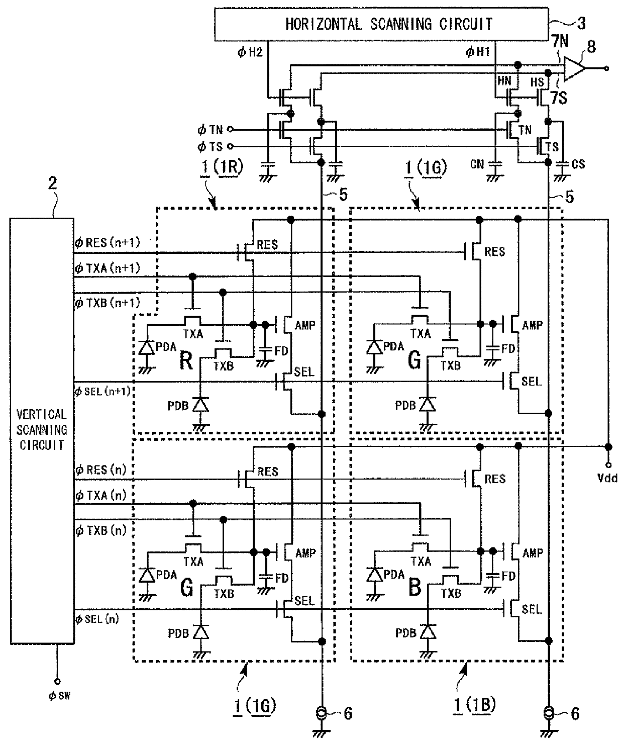
[0043]FIG. 1 is a circuit diagram schematically illustrating the structure adopted in the solid-state image sensor achieved in the first embodiment of the present invention. The solid-state image sensor in the embodiment is a CMOS solid-state image sensor.

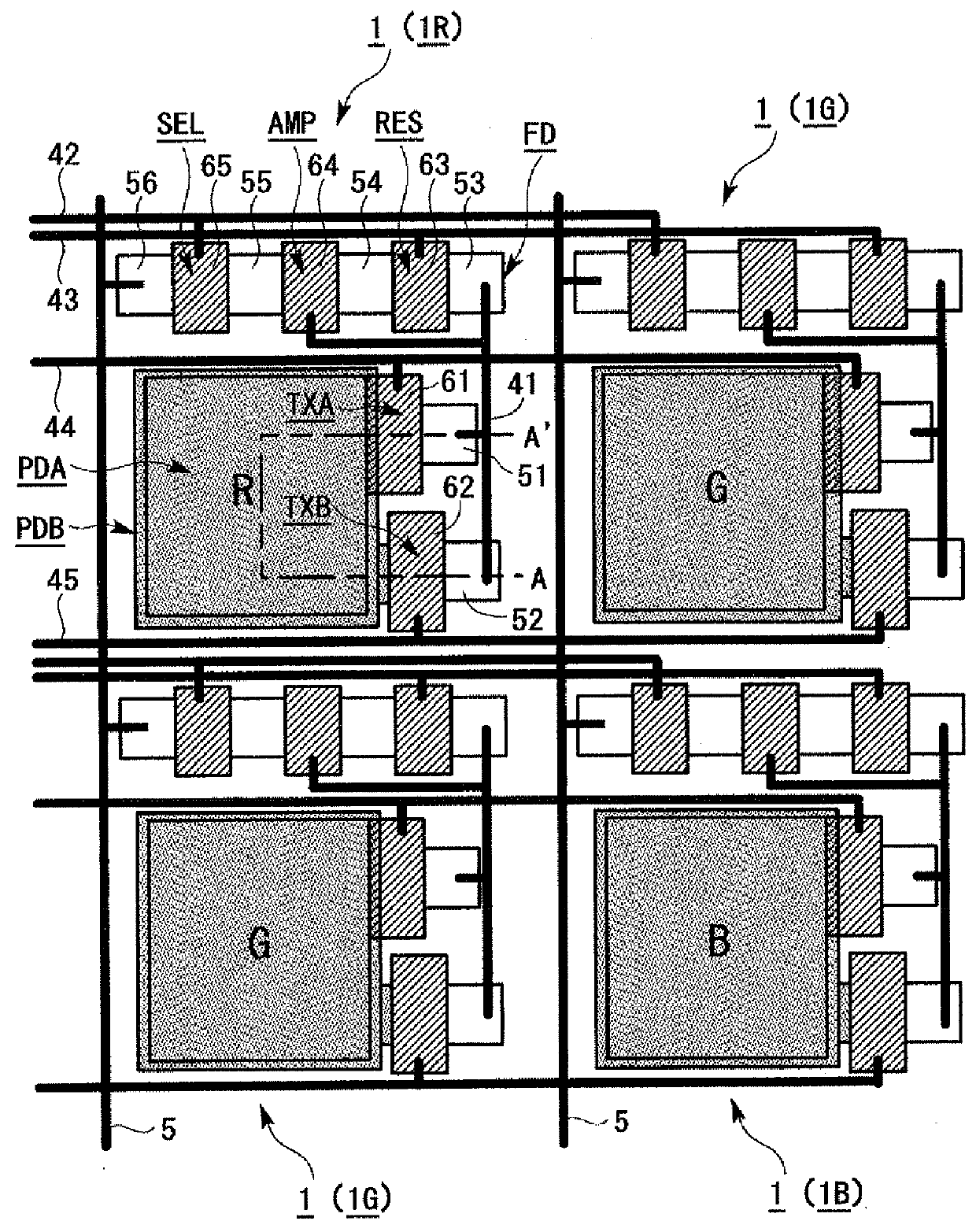
[0044]The solid-state image sensor in the embodiment comprises a plurality of pixels 1 arrayed in a two-dimensional pattern (the figure only shows 2×2 pixels 1), a vertical scanning circuit 2, a horizontal scanning circuit 3, vertical signal lines 5, a constant current source 6, a first horizontal signal line 7S, a second horizontal signal line 7N and a differential output amplifier 8. The vertical signal lines 5 are each disposed in correspondence to a column of pixels 1. The constant current source 6 is connected to the individual vertical signal lines 5. Through the first horizontal signal line 7S, optical signals containing optical information resulting from photoelectric conversion executed at the pixels 1, are transmitted. Th...

second embodiment

[0088]FIG. 10 presents a timing chart of the operation executed in the solid-state image sensor assuming a third operation mode in the second embodiment of the present invention.

[0089]The following explanation focuses on the feature of the second embodiment distinguishing it from the first embodiment. The following feature of the solid-state image sensor in the embodiment differentiates it from the solid-state image sensor achieved in the first embodiment. The vertical scanning circuit 2 in the first embodiment outputs the various control signals explained earlier so as to selectively execute operation in the first operation mode, as shown in FIG. 8, or in the second operation mode, as shown in FIG. 9, in response to an operation mode selection signal ØSW. In the second embodiment, the vertical scanning circuit 2 outputs the various control signals so as to selectively execute operation in the first operation mode, as shown in FIG. 8, or in the third operation mode, as shown in FIG....

third embodiment

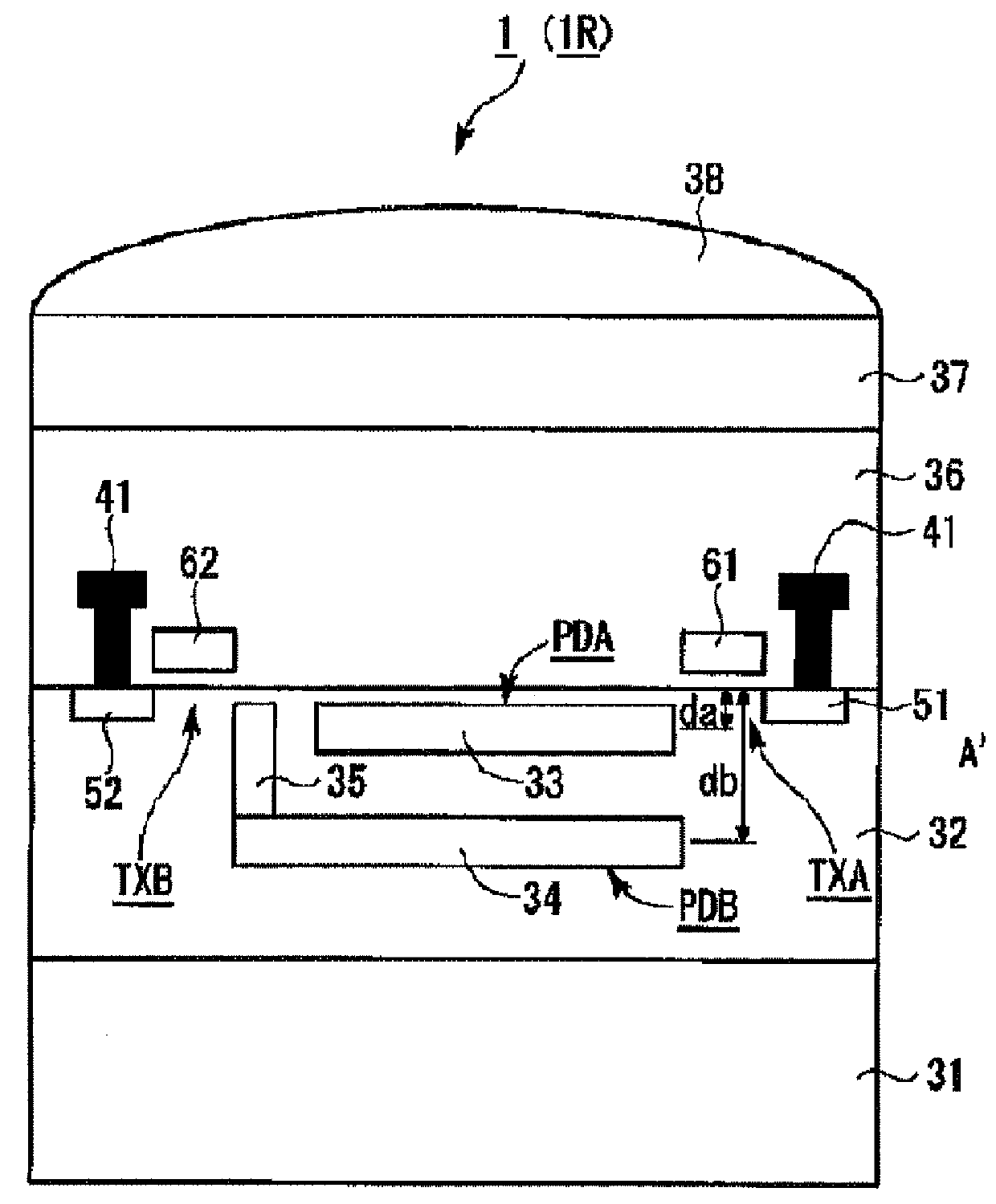
[0098]The following feature of the solid-state image sensor achieved in the third embodiment of the present invention differentiates it from the solid-state image sensor in the first embodiment. In the solid-state image sensor in the first embodiment, two conditions, i.e., a first condition whereby a uniform depth da is assumed for the charge storage layers 33 of all the pixels 1 (1R, 1G and 1B) and a second condition whereby a uniform depth db is assumed for the charge storage layers 34 at all pixels 1 (1R, 1G and 1B) are both satisfied. In contrast, the depths da and db at the individual pixels 1 (1R, 1G and 1B) are set by ensuring that at least either the first condition or the second condition is not satisfied in this embodiment. In other words, the third embodiment differs from the first embodiment in that the depths da and db are set so as to satisfy requirements (1) and (2) below.

[0099](1) Better uniformity is achieved with respect to the intervals between the peaks PBA, PBB,...


PUM


Abstract

A solid-state image sensor includes: four or more photoelectric conversion units having spectral sensitivity characteristics different from one another; an amplifier unit disposed in correspondence to each group of photoelectric conversion units among N groups (N represents an integer less than a quantity of the four or more photoelectric conversion units and equal to or greater than one), the four or more photoelectric conversion units being divided into the N groups; and transfer units, each disposed in correspondence to one of the four or more photoelectric conversion units, which transfer a signal generated at the photoelectric conversion unit to the amplifier unit disposed for the group to which the photoelectric conversion unit belongs.

Description

INCORPORATION BY REFERENCE[0001]The disclosure of the following priority application is herein incorporated by reference:Japanese Patent Application No. 2009-185343 filed Aug. 8, 2009Japanese Patent Application No. 2010-174881 filed Aug. 3, 2010BACKGROUND OF THE INVENTION[0002]1. Field of the Invention[0003]The present invention relates to a solid-state image sensor.[0004]2. Description of Related Art[0005]The pixels in a standard solid-state image sensor in the related art may each include a single photoelectric conversion unit, with a color filter in one of three colors (R, G and B) disposed on each pixel. In such a solid-state image sensor, an R color signal, a G color signal or a B color signal is obtained from a given photoelectric conversion unit.[0006]The solid-state image sensor disclosed in Japanese Laid Open Patent Publication No. 2006-165362 is distinct from the image sensor described above in that at least some of its pixels are equipped with two or more photoelectric co...

Claims


Application Information

Patent Timeline
Patent Type & Authority Patents(United States)
IPC IPC(8): H01L27/00G01J1/44H01L27/146H04N9/04H04N23/12
CPCH01L27/14647H01L27/14641H04N9/045H01L27/14621H01L27/14627
Inventor NARUI, TADASHI
Owner NIKON CORP
Learn More