Method for manufacturing a waveguide including a semi-conducting junction

a semi-conducting junction and waveguide technology, applied in the field of microelectronics and optoelectronics, can solve the problems of increasing the manufacturing cost of such a waveguide, unable to obtain a vertical junction, and not being able to activate, so as to achieve accurate junction positioning

Active Publication Date: 2016-09-06
COMMISSARIAT A LENERGIE ATOMIQUE ET AUX ENERGIES ALTERNATIVES
View PDF6 Cites 0 Cited by
  • Summary
  • Abstract
  • Description
  • Claims
  • Application Information

AI Technical Summary

Benefits of technology

[0018]The aim of the invention is to resolve this drawback and the object thereof is to make possible to provide a waveguide at least one optical property of which can be modified, without requiring, to provide the waveguide with an accurate positioning of the junction in proximity to the centre of the waveguide, any significant additional cost related to the alignment of the mask.
[0026]With such a method, positioning the junction with respect to the first side wall of the waveguide is determined by the diffusion length of the second conductivity-type dopants in the first part. Thus, with an adapted diffusion of the second conductivity-type dopants, it is possible to achieve an optimum positioning of the junction with respect to the first wall and therefore to the centre of the waveguide. Such a method then enables the junction to be positioned in proximity to the centre of the waveguide. Moreover, since the diffusion occurs from the vertical interface between the first and the second part, the final orientation of the junction in the waveguide is also vertical, that is transverse with respect to the support of the waveguide.
[0027]It is also to be noted that the optimum positioning and orientation of the junction with respect to the centre of the waveguide does not lead to any significant additional cost as is the case for the prior art methods since the alignment of the mask for etching is mainly achieved by reusing the protection used during implanting.
[0032]With an implantation of second conductivity-type dopants during the step of implanting, it is possible to provide an optimum placing of the semiconducting junction through a step of diffusing consisting in a simple annealing enabling a maximum diffusion of the second conductivity-type dopants to be provided.
[0035]The use of two protecting elements, a first mask protecting the area of the first part intended to form the waveguide and a second mask protecting the remainder of the first part, enables a simplified use of the protection during the step of partial etching. Indeed, a selective removal of the second protecting element enables an adequate protection to be achieved to protect the area intended to form the waveguide during the step of partial etching.
[0044]Such a method makes it possible to enjoy advantages related to the method for manufacturing a waveguide according to the invention.

Problems solved by technology

This alignment, due to the sizing of the waveguide and because the junction must be accurately positioned with respect to the centre of the waveguide, is relatively complex to set up and drastically increases the manufacturing cost of such a waveguide.
Nevertheless, if such a method enables a good control of the positioning of the junction with respect to the waveguide without drastically increasing the manufacturing cost, the junction inevitably lies in proximity to a wall of the waveguide and is therefore remote from the centre of the waveguide.
It is moreover to be noted that diffusing the dopants during the step of activating does not allow a vertical junction to be obtained.

Method used


Image

  • Method for manufacturing a waveguide including a semi-conducting junction
  • Method for manufacturing a waveguide including a semi-conducting junction
  • Method for manufacturing a waveguide including a semi-conducting junction

Examples


Embodiment Construction

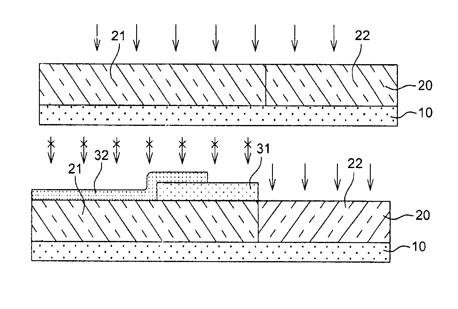
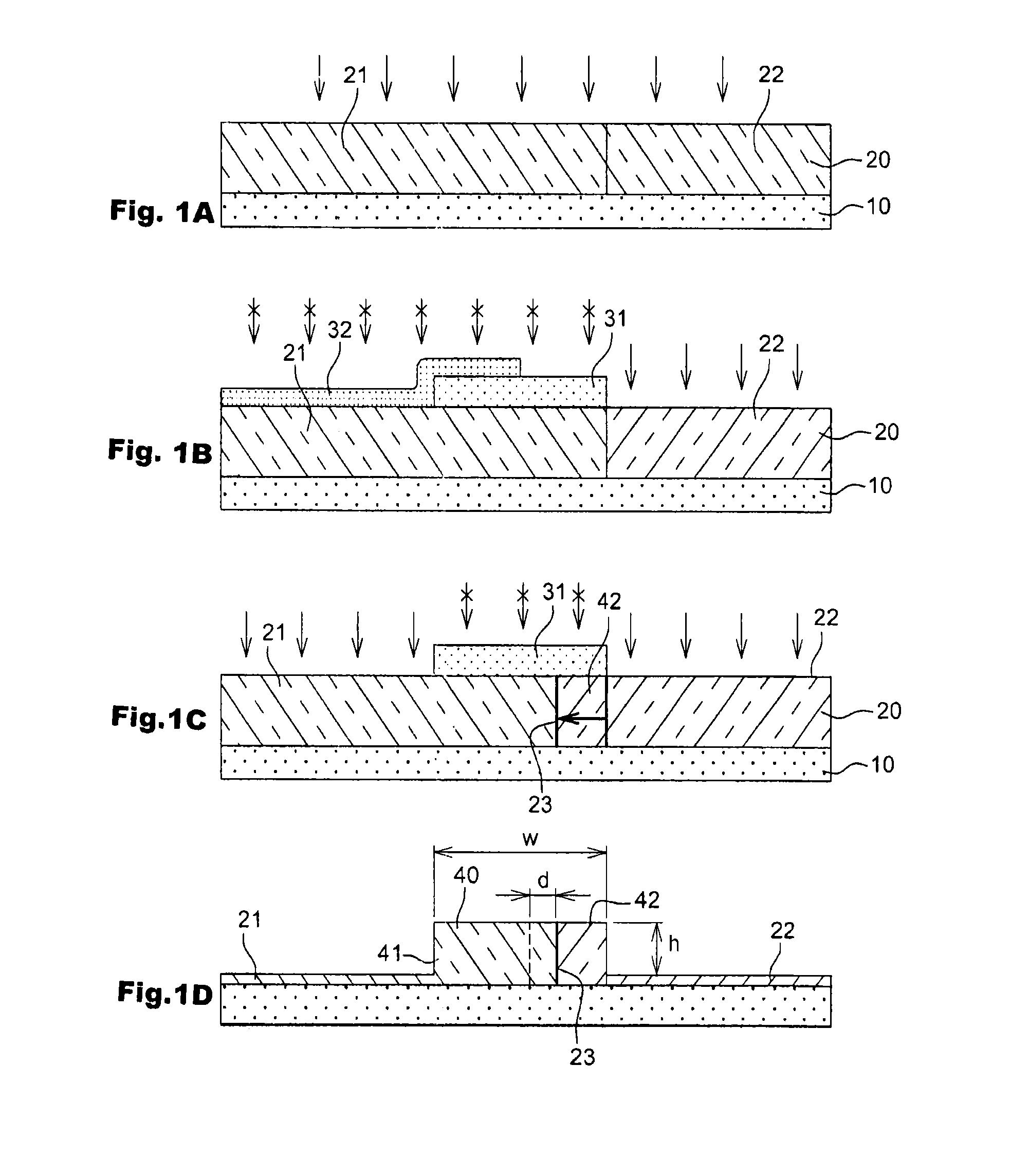
[0055]FIGS. 1A to 1D illustrate the main steps for manufacturing a waveguide 40 according to the invention having optical properties which can be modulated and which is able to be comprised in a component such as a Mach-Zehnder-type or ring-type optical modulator.

[0056]Thus, according to the principle of the invention illustrated schematically and in a transverse cross-section in FIG. 1D, a component 1 having such a waveguide 40 includes a support 10, such as here, a silicon substrate on which an insulator layer is disposed according to the silicon-on-insulator principle, more commonly known as the acronym SOI, only the insulating layer being represented.

[0057]Said support 10 comprises a semiconducting layer 20 having a first part 21 mainly of a first conductivity type and a second part 22 of a second conductivity type adjacent to the first part 21, the first part having, in proximity to the second part 22, a portion of the second conductivity type so that a semiconducting junction ...


PUM

PropertyMeasurementUnit
heightaaaaaaaaaa
heightaaaaaaaaaa
widthaaaaaaaaaa

Abstract

The invention relates to a method for manufacturing a waveguide (40) including a semiconducting junction (23). The method comprises the following steps: providing a support (10) comprising a semiconducting layer (20) having a first part (21) of a first conductivity type ; protecting the first part ; selectively implanting a second conductivity-type dopants in a second part (22) of the semiconducting layer (20) adjacent to the first part (21, 221). The concentration of second conductivity-type dopants in the second part (22, 222) is greater than the one of first conductivity-type dopants in the first part (21, 221). The method further comprises the steps of: diffusing second conductivity-type dopants in the first part (21, 221) to form a semiconducting junction (23, 223) in the first part (21, 221), and partially etching the semiconducting layer (20, 200) to form the waveguide (40, 240) in the first part (21, 221), the protection of the first part (21, 221) being used so that the semiconducting junction (23, 223) is included in the waveguide (40, 240).

Description

TECHNICAL FIELD[0001]The invention relates to the fields of microelectronics and optoelectronics and more particularly relates to the methods for manufacturing semiconducting structures for integrated optoelectronics, such as optical modulators.STATE OF PRIOR ART[0002]The optical modulators, such as the Mach-Zehnder or resonant ring-type modulators, usually integrate a waveguide the optical properties of which can be modulated.[0003]Such a waveguide the optical properties of which can be modulated is usually provided by a semiconducting waveguide into which a semiconducting junction has previously being included. Indeed, the optical properties of such a waveguide, such as the effective index, can be easily modulated by adequately polarizing the semiconducting junction.[0004]A conventional method for manufacturing such a waveguide consists in implementing the following steps:[0005]providing a support including a semiconducting layer, at least one first part of the layer having a firs...

Claims


Application Information

Patent Timeline
Patent Type & Authority Patents(United States)
IPC IPC(8): H01L21/00G02B6/134G02B6/136G02F1/025G02F1/225G02F1/21
CPCG02B6/1347G02B6/136G02B6/1342G02F1/025G02F1/2257G02F2001/212H01L2223/6627H01L2223/6633G02B6/12004G02F1/212
Inventor FOURNIER, MARYSEFOWLER, DAIVIDGRELLIER, EDOUARDIOTTI, LORENZO
Owner COMMISSARIAT A LENERGIE ATOMIQUE ET AUX ENERGIES ALTERNATIVES
Why Eureka
Try Eureka