Method of manufacturing semiconductor and exposure system

a manufacturing method and exposure system technology, applied in the direction of microlithography exposure apparatus, printers, instruments, etc., can solve the problems of serious affecting productivity and waste of production line resources, requiring further detection or rework of the warning target, and requiring unnecessary rework, so as to reduce the frequency of false warnings, ensure product quality, and monitor the accuracy of alignmen

Active Publication Date: 2016-09-20
MACRONIX INT CO LTD
View PDF17 Cites 0 Cited by
  • Summary
  • Abstract
  • Description
  • Claims
  • Application Information

AI Technical Summary

Benefits of technology

[0034]Based on above, the method of manufacturing semiconductor and the exposure system provided by the invention are capable of calculating the monitor parameter group after the patterned photoresist layer is exposed to obtain the virtual parameter, and comparing the virtual parameter with the set reference value, so as to monitor the accuracy of the alignment to ensure product quality. The method of manufacturing semiconductor is capable of reducing a frequency of the false warning sent by an exposure machine to avoid unnecessary reworks and effectively monitoring alignment behaviors between layers.

Problems solved by technology

In this case, the wafer to which the warning is targeted may require further detection or reworks.
However, if a range for setting the control values is improper or requires frequent adjustments, which will cause false warnings and unnecessary reworks to seriously influence productivity and waste resources on production line.
Therefore, how to effectively monitor the alignment behaviors between layers while reducing a frequency of the false warning is an important issue to be discussed in the field.

Method used


Image

  • Method of manufacturing semiconductor and exposure system
  • Method of manufacturing semiconductor and exposure system
  • Method of manufacturing semiconductor and exposure system

Examples


first embodiment

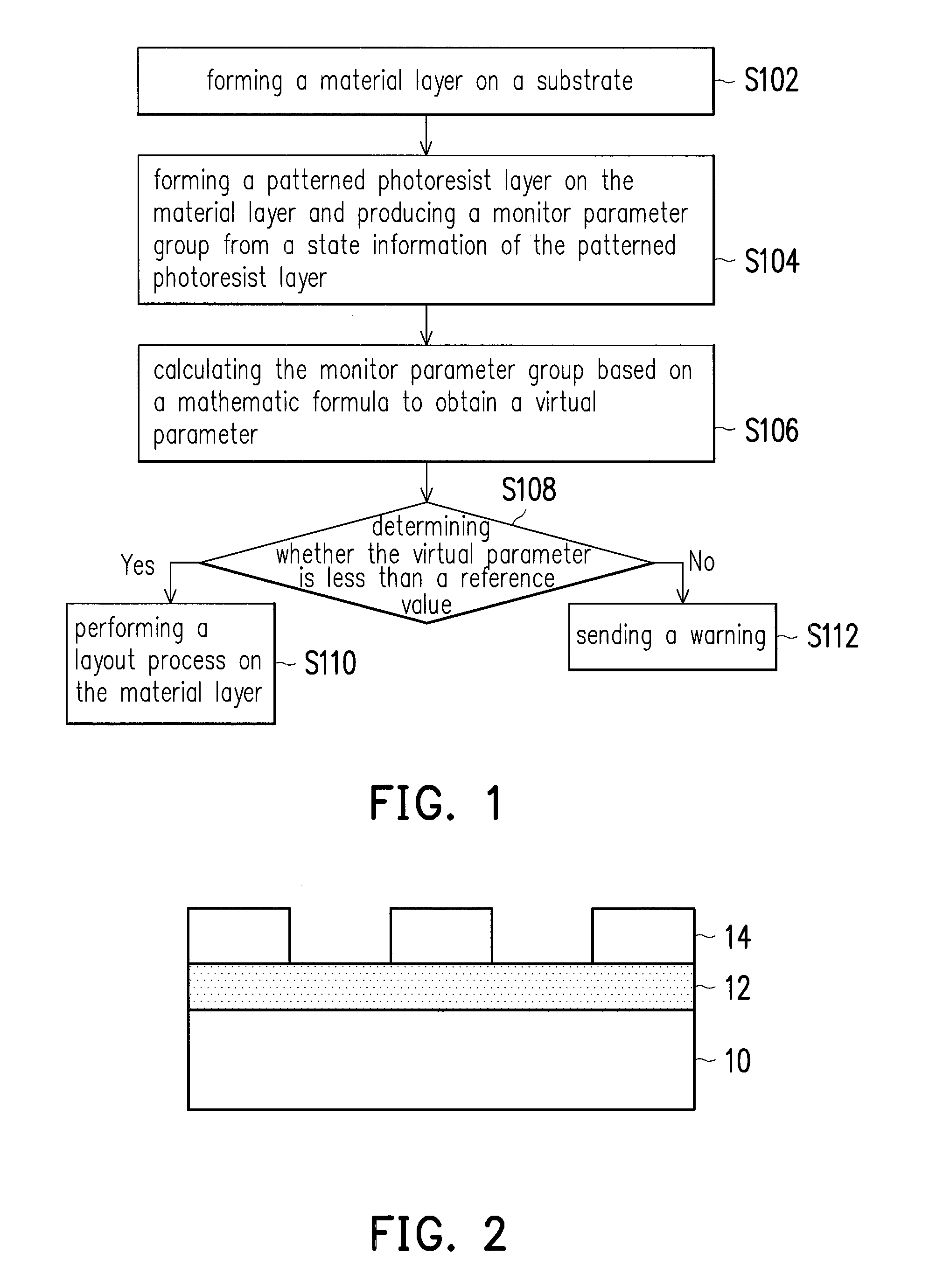
[0055]The flowchart illustrating the method of manufacturing semiconductor of the invention is as shown by steps S102 to S112 in FIG. 1. In step S102, a material layer 12 is formed on a substrate 10. Next, in step S104, a patterned photoresist layer 14 is formed on the material layer 12 and a monitor parameter group is produced from a state information of the patterned photoresist layer 14. Subsequently, in step S106, the monitor parameter group is calculated based on a mathematic formula to obtain a virtual parameter. Then, in step S108, whether the virtual parameter is less than a reference value is determined. Thereafter, in step S110, a layout process is performed on the material layer 12 when the virtual parameter is less than the reference value. Additionally, in step S112, a warning is sent when the virtual parameter is greater than the reference value. Detailed steps and description for the above are provided as follows.

[0056]Referring to FIG. 1 and FIG. 2, in step S102, th...

second embodiment

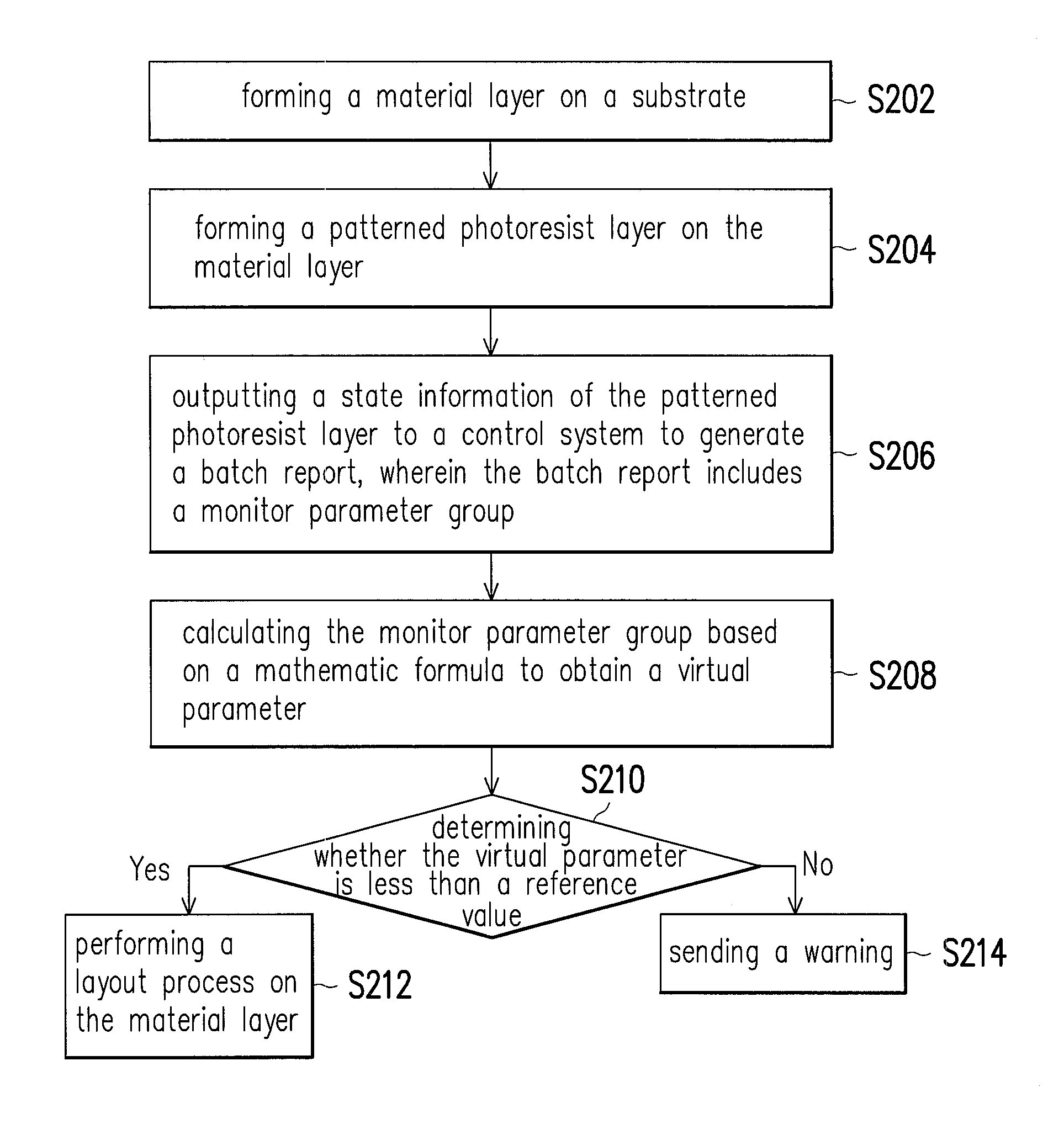
[0073]FIG. 5 is a flowchart illustrating a method of manufacturing semiconductor of the invention.

[0074]The flowchart illustrating the method of manufacturing semiconductor according to second embodiment of the invention is as shown by steps S202 to S214 in FIG. 5. In step S202, a material layer is formed on a substrate. Next, in step S204, a patterned photoresist layer is formed on the material layer. Then, in step S206, a state information of the patterned photoresist layer is outputted to a control system to generate a batch report, wherein the batch report includes a monitor parameter group. Subsequently, in step S208, the monitor parameter group is calculated based on a mathematic formula to obtain a virtual parameter. Then, in step S210, whether the virtual parameter is less than a reference value is determined. Thereafter, in step S212, a layout process is performed on the material layer 12 when the virtual parameter is less than the reference value. Additionally, in step S2...


PUM

PropertyMeasurementUnit
semiconductoraaaaaaaaaa
rotationaaaaaaaaaa
rotation factoraaaaaaaaaa

Abstract

A method of manufacturing semiconductor and an exposure system are provided. The method includes the following step. A material layer is formed on a substrate. A patterned photoresist layer is formed a on the material layer and a monitor parameter group is produced from a state information of the patterned photoresist layer. The monitor parameter group is calculated based on a mathematic formula to obtain a virtual parameter. Whether the virtual parameter is less than a reference value is determined. A layout process is performed on the material layer when the virtual parameter is less than the reference value.

Description

CROSS-REFERENCE TO RELATED APPLICATION[0001]This application claims the priority benefit of Taiwan application serial no. 103112314, filed on Apr. 2, 2014. The entirety of the above-mentioned patent application is hereby incorporated by reference herein and made a part of this specification.BACKGROUND OF THE INVENTION[0002]1. Field of the Invention[0003]The invention relates to a manufacturing method and a processing system, and more particularly, relates to a method of manufacturing semiconductor and an exposure system.[0004]2. Description of Related Art[0005]With increasing IC integration level, dimensions of patterns are also gradually reduced day by day, thus, how to align multiple layers in a device has become one of important factors in manufacturing semiconductor. In other words, each layer must be accurately aligned to the others, so that circuits formed therein may match layout patterns and operate normally. Alignment is a critical step in a lithography process because a wa...

Claims


Application Information

Patent Timeline
Patent Type & Authority Patents(United States)
IPC IPC(8): G03B27/68G03F7/20
CPCG03F7/70141G03F7/70633
Inventor WU, SHIH-RUNGLAI, RUI-MING
Owner MACRONIX INT CO LTD
Why Eureka
Try Eureka