Semiconductor memory device improving threshold voltage of unselected memory block and operating method thereof

a memory device and semiconductor technology, applied in the field of semiconductor memory devices, can solve the problems of constant source of power, non-volatile memory devices operating at relatively low write and read speeds, and inability to retain stored data, etc., and achieve the effect of improving the threshold voltage distribution

Active Publication Date: 2016-10-11
SK HYNIX INC
View PDF15 Cites 4 Cited by
  • Summary
  • Abstract
  • Description
  • Claims
  • Application Information

AI Technical Summary

Benefits of technology

[0009]An embodiment is directed to a semiconductor memory device capable of improving the threshold voltage distribution of an unselected memory block of at least two memory blocks sharing a single row decoder during a read operation of the semiconductor, and an operating method thereof.

Problems solved by technology

Volatile memory devices operate at high write and read speeds, but they are unable to retain their stored data when their power supply is interrupted.
Non-volatile memory devices operate at relatively low write and read speeds, but they may retain the stored data without a constant source of power.

Method used


Image

  • Semiconductor memory device improving threshold voltage of unselected memory block and operating method thereof
  • Semiconductor memory device improving threshold voltage of unselected memory block and operating method thereof
  • Semiconductor memory device improving threshold voltage of unselected memory block and operating method thereof

Examples


Embodiment Construction

[0021]Hereinafter, various exemplary embodiments will be described in detail with reference to the accompanying drawings. In the drawings, thicknesses and lengths of components may be exaggerated for convenience of illustration. In the following description, a detailed explanation of related functions and constitutions may be omitted for simplicity and conciseness of explanation. Like reference numerals refer to like elements throughout the specification and drawings.

[0022]Furthermore, ‘connected / coupled’ represents that one component is directly electrically coupled to another component or indirectly electrically coupled through another component. A singular form may include a plural form as long as it is not specifically mentioned in a sentence. Furthermore, ‘include / comprise’ or ‘including / comprising’ used in the specification represents that one or more components, steps, operations, and elements exist or have been added.

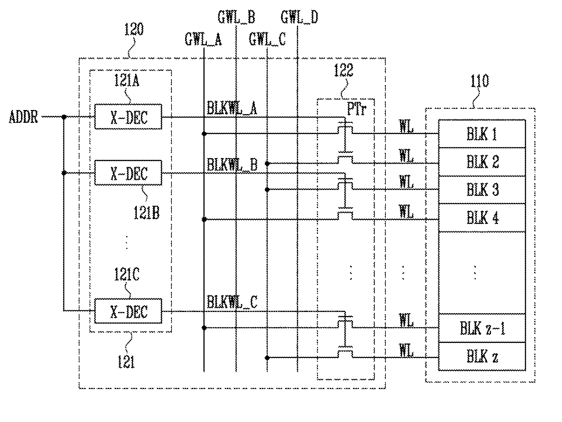
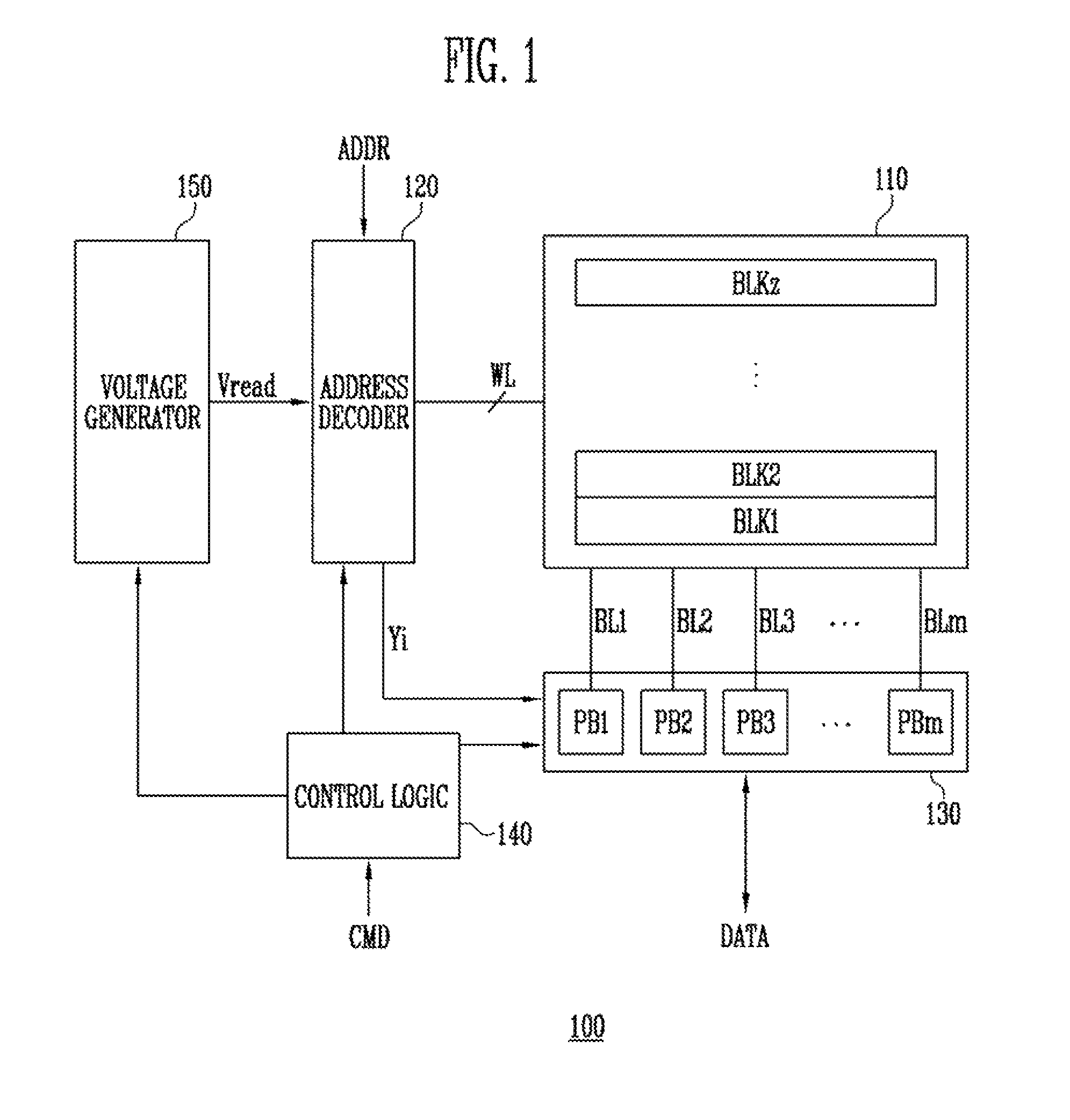
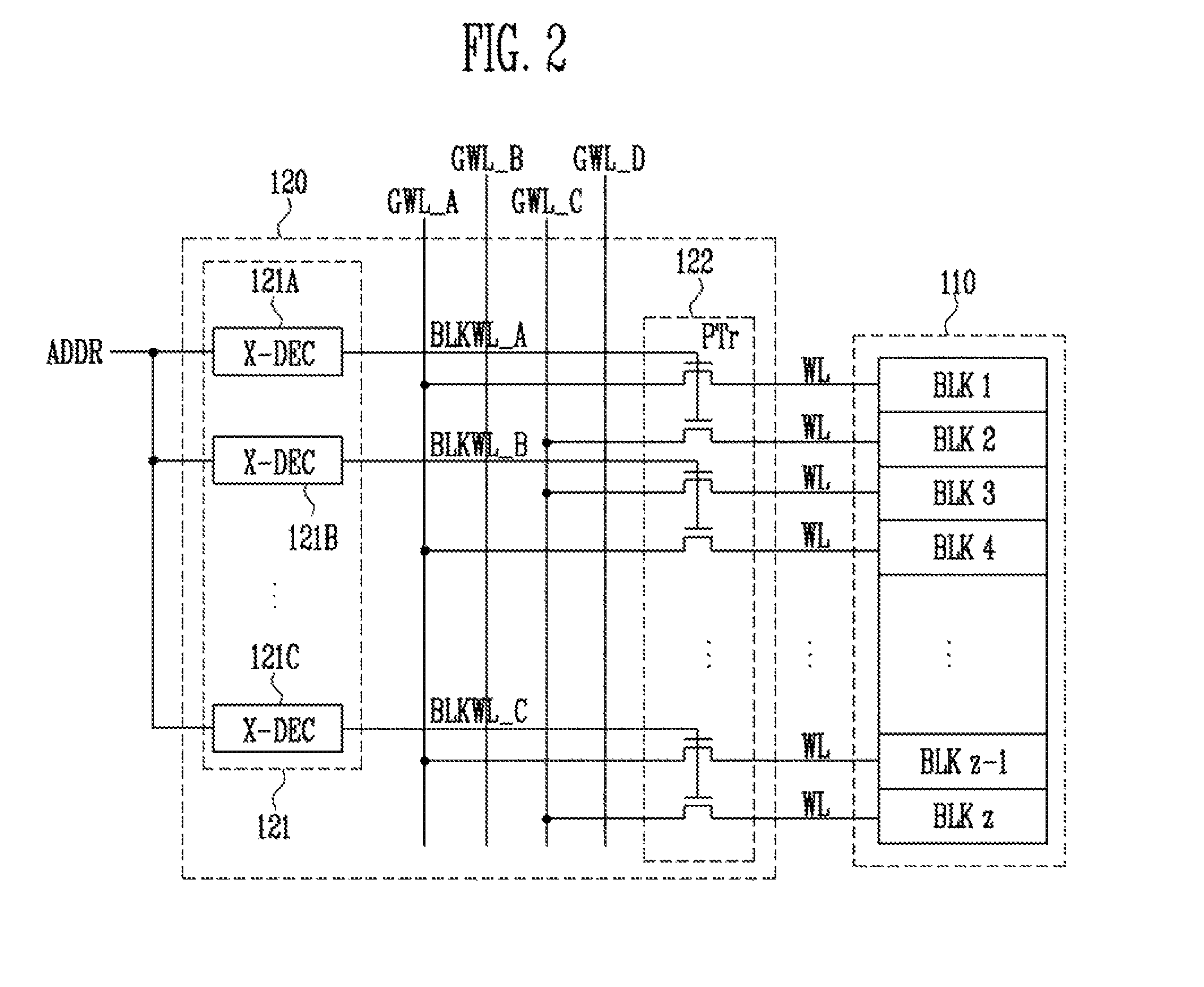
[0023]FIG. 1 is a block diagram illustrating a semiconduct...


PUM


Abstract

The present invention relates to a semiconductor memory device and an operating method thereof. The semiconductor memory device may include at least two memory blocks sharing a row decoder, and a peripheral circuit performing a read operation on a selected memory block, between the at least two memory blocks, wherein the peripheral circuit applies a discharge voltage to an unselected memory block, between the at least two memory blocks, for a preset time after a period in which a read voltage is applied to the selected memory block is terminated.

Description

CROSS-REFERENCE TO RELATED APPLICATION[0001]The present application claims priority to Korean patent application number 10-2014-0164327, filed on Nov. 24, 2014, the entire disclosure of which is herein incorporated in its entirety by reference.BACKGROUND[0002]1. Field of Invention[0003]Various exemplary embodiments relate generally to an electronic device, and more particularly, to a semiconductor memory device and an operating method thereof.[0004]2. Description of Related Art[0005]Semiconductor memory devices are typically categorized into volatile memory devices and non-volatile memory devices.[0006]Volatile memory devices operate at high write and read speeds, but they are unable to retain their stored data when their power supply is interrupted. Non-volatile memory devices operate at relatively low write and read speeds, but they may retain the stored data without a constant source of power. Examples of non-volatile memory devices include Read Only Memory (ROM), Mask ROM (MROM)...

Claims


Application Information

Patent Timeline
Patent Type & Authority Patents(United States)
IPC IPC(8): G11C16/08G11C16/04G11C16/26
CPCG11C16/08G11C16/0483G11C16/26
Inventor AN, CHI WOOK
Owner SK HYNIX INC
Why Eureka
Try Eureka