Chip resistor and method for making the same

a chip resistor and chip technology, applied in the manufacture of resistors, resistor details, resistors, etc., can solve the problems of insufficient resistance of conventional resistors, insufficient thickness of metal resistor elements to ensure proper mechanical strength of devices, etc., to achieve the effect of increasing resistan

Active Publication Date: 2016-12-06
ROHM CO LTD
View PDF14 Cites 9 Cited by
  • Summary
  • Abstract
  • Description
  • Claims
  • Application Information

AI Technical Summary

Benefits of technology

[0005]The present invention has been proposed under the circumstances described above. It is therefore an object of the present invention to provide a chip resistor having increased resistance without compromising the mechanical strength of the device.

Problems solved by technology

In this chip resistor, however, the metal resistor element cannot be sufficiently small in thickness for ensuring proper mechanical strength of the device.
Thus, the resistance of the conventional resistor cannot be made sufficiently high.

Method used


Image

  • Chip resistor and method for making the same
  • Chip resistor and method for making the same
  • Chip resistor and method for making the same

Examples


Embodiment Construction

[0069]Embodiments of the present invention are described below with reference to the accompanying drawings.

[0070]An embodiment of the present invention is described below with reference to FIGS. 1-25.

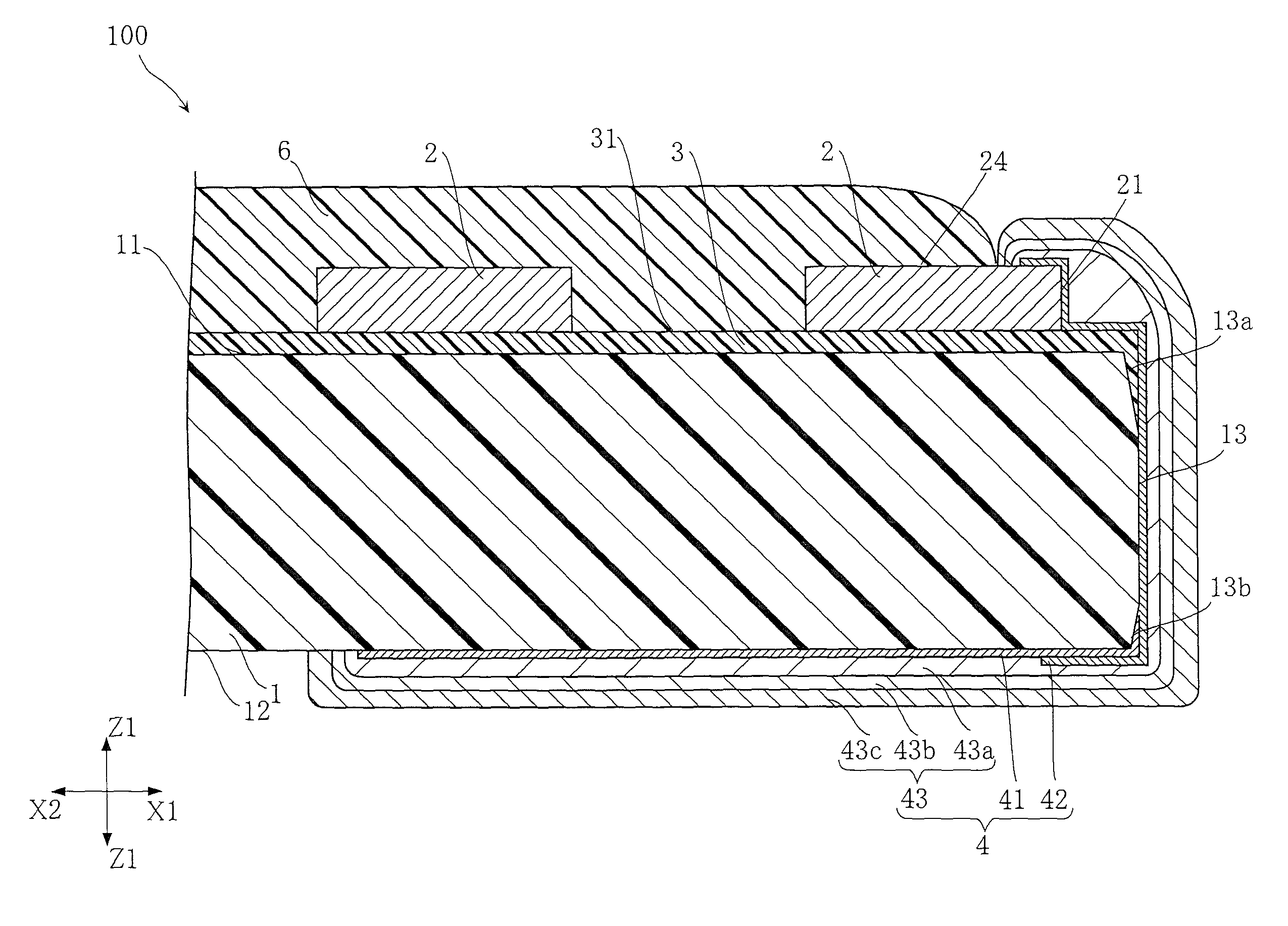
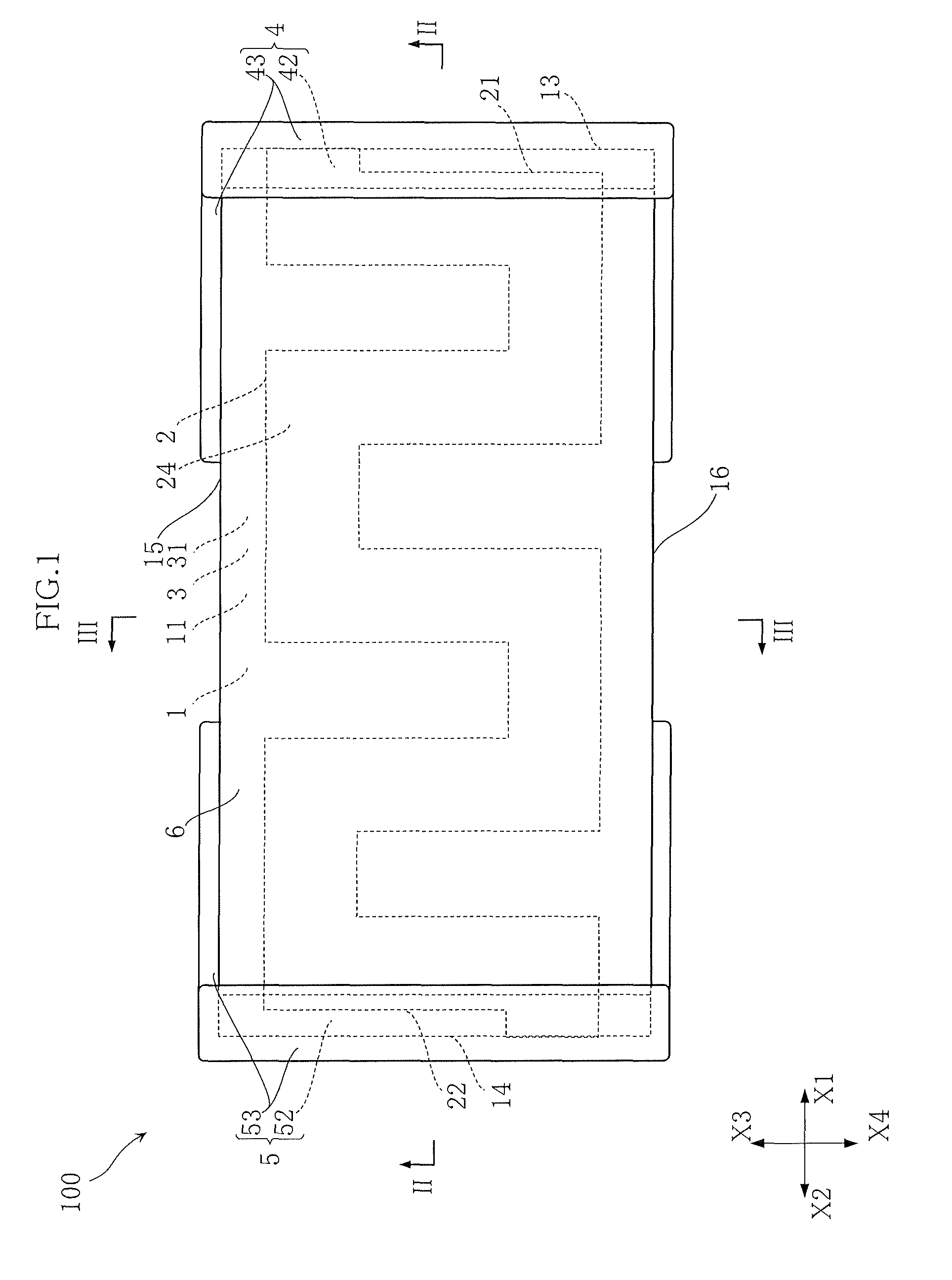
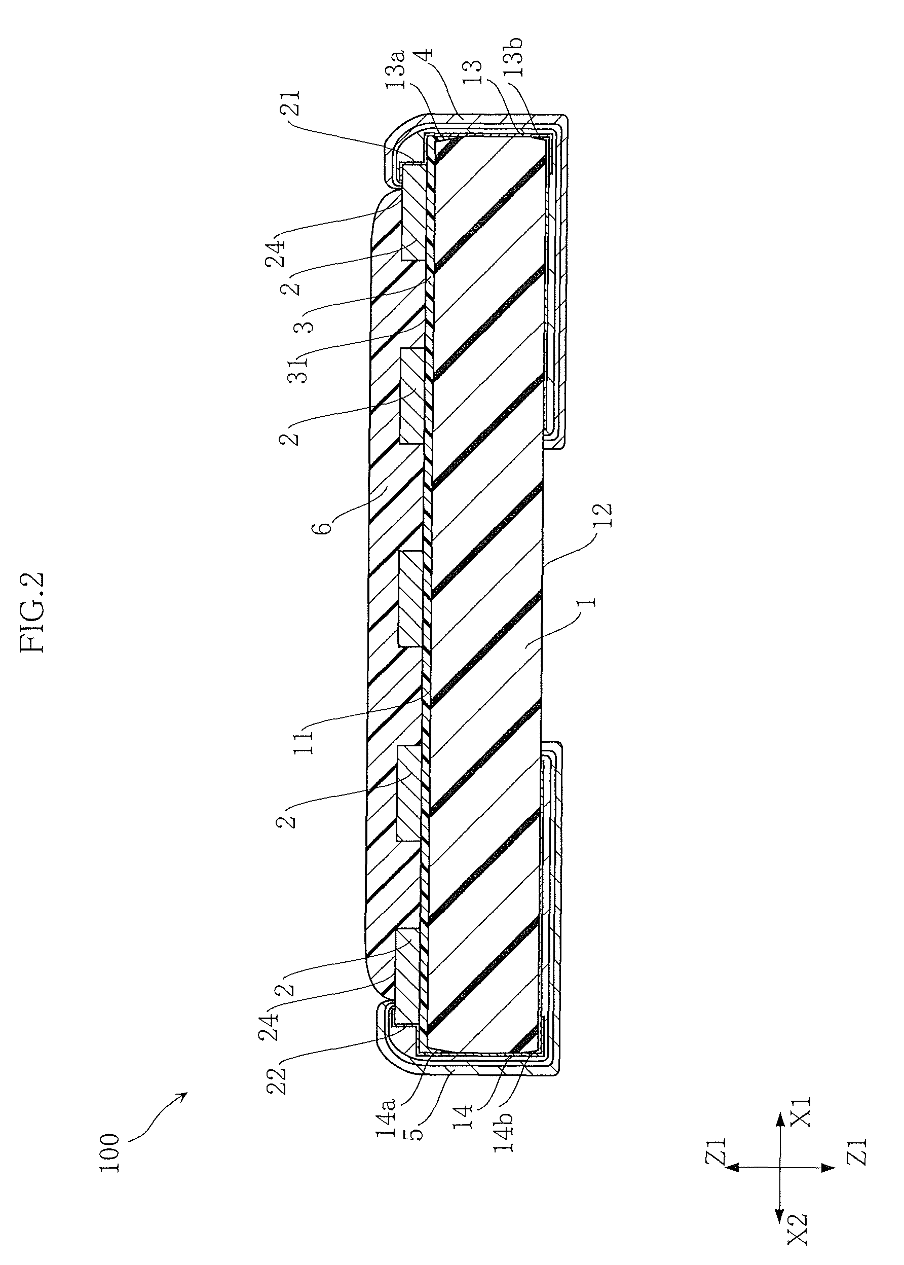
[0071]The chip resistor 100 shown in these figures includes a substrate 1, a resistor element 2, a bonding layer 3, a first electrode 4, a second electrode 5 and a protective film 6.

[0072]The substrate 1 is in the form of a plate and has insulating properties. For instance, the substrate 1 is made of a ceramic material or a resin. Examples of the ceramic material include Al2O3, AlN and SiC. In order that heat generated at the resistor element 2 can easily dissipate to the outside of the chip resistor 100, it is preferable to use a material having a high thermal conductivity for forming the substrate 1. The substrate 1 has a substrate obverse surface 11, a substrate reverse surface 12, a first substrate side surface 13, a second substrate side surface 14, a third substrate side surface 1...


PUM

PropertyMeasurementUnit
thicknessaaaaaaaaaa
thicknessaaaaaaaaaa
thermal conductivityaaaaaaaaaa

Abstract

A chip resistor includes an insulating substrate, a resistor element arranged on the obverse surface of the substrate, a bonding layer provided between the resistor element and the substrate, a first electrode connected to the resistor element, and a second electrode connected to the resistor element. The second electrode is deviated from the first electrode in a direction perpendicular to the thickness direction of the substrate. The substrate includes a side surface between the obverse surface and the reverse surface. The first electrode covers the resistor element, and also the side surface and the reverse surface of the substrate.

Description

BACKGROUND OF THE INVENTION[0001]1. Field of the Invention[0002]The present invention relates to a chip resistor and a method for making a chip resistor.[0003]2. Description of the Related Art[0004]Conventionally, chip resistors for use in electronic equipment are known. For instance, JP-A-2009-218552 discloses a chip resistor that includes a resistor element made of metal and two electrodes provided on the resistor element. In this chip resistor, however, the metal resistor element cannot be sufficiently small in thickness for ensuring proper mechanical strength of the device. Thus, the resistance of the conventional resistor cannot be made sufficiently high.SUMMARY OF THE INVENTION[0005]The present invention has been proposed under the circumstances described above. It is therefore an object of the present invention to provide a chip resistor having increased resistance without compromising the mechanical strength of the device.[0006]According to a first aspect of the present inve...

Claims


Application Information

Patent Timeline
Patent Type & Authority Patents(United States)
IPC IPC(8): H01C1/012H01C1/08H01C17/00H01C1/14
CPCH01C17/006H01C1/08H01C1/14Y10T29/49099Y10T156/10
Inventor HARADA, KENICHIYONEDA, MASAKI
Owner ROHM CO LTD
Why Eureka
Try Eureka