Methods and circuitry to provide common mode transient immunity

a common mode and transient immunity technology, applied in the field of methods and circuitry to provide to achieve the effect of accurate cancellation of corresponding and higher common mode transient immunity

Active Publication Date: 2017-01-17
INFINEON TECH AMERICAS CORP
View PDF3 Cites 2 Cited by
  • Summary
  • Abstract
  • Description
  • Claims
  • Application Information

AI Technical Summary

Benefits of technology

[0006]A high-voltage, high slew-rate CMTI event can be seen by the isolation barrier in such a way that the CM bias points of the various interface circuits maintain proper linear operation so as to avoid gross distortion of the signaling interface. This implies a low CM impedance input on the receiver interface to counter the loading of the coupling capacitance during a CMTI event. However, to maintain good receive signal amplitude for robust signal-to-noise, the differential interface must offer minimal signal attenuation which implies large differential-mode (DM) impedance. Therefore, one desirable goal as further described herein is to supply a mechanism to maintain large DM impedance (for minimal DM attenuation) and small CM impedance (for minimal bias point excursions during CMTI events).
[0015]The monitor circuit derives an adjustment signal based on detected presence of the second common mode transient signal present on the second communication path. The gain modifier circuit modifies a gain setting that is applied to subsequent derived adjustment signals produced by the monitor circuit to provide better common mode transient immunity. In other words, the first common mode transient signal may not precisely match the second common mode transient signal due to electrical parameter (e.g., capacitance, impedance, differential mode, etc.) mismatch in each of the paths. The modified gain is applied to the subsequent adjustment signals during subsequent operation so that the generated adjustment signals (representative of the common mode transient on the replica communication path) more closely match the common mode induced transient signals on the first communication path, thus providing better common mode transient immunity.

Problems solved by technology

For high slew rate transients (>35 kV / us to levels in excess of 100 kV / us), CM impedance control is still paramount and more challenging, but a second order effect due to common-mode to differential-mode conversion due to device mismatch becomes a challenge to address.

Method used


Image

  • Methods and circuitry to provide common mode transient immunity
  • Methods and circuitry to provide common mode transient immunity
  • Methods and circuitry to provide common mode transient immunity

Examples


Embodiment Construction

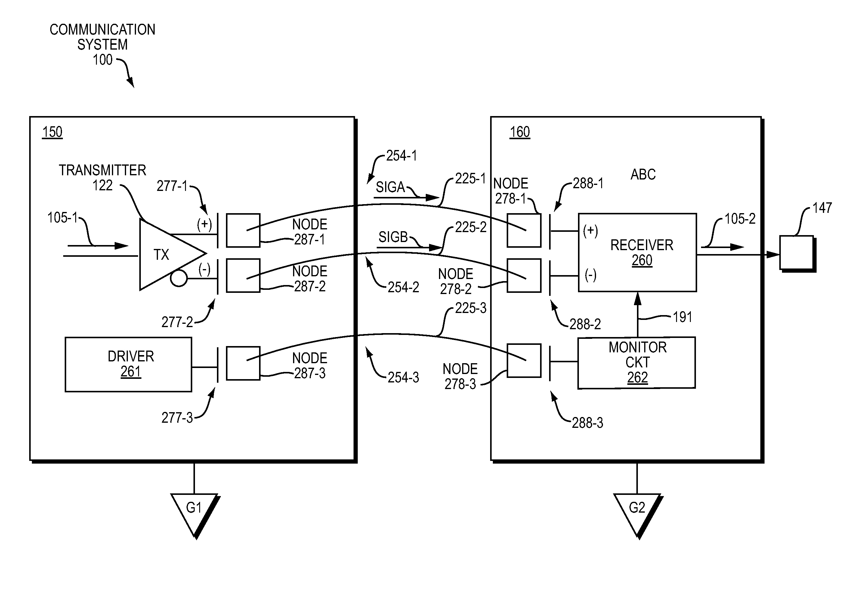
[0029]As further described below, embodiments herein include a replica communication path and monitor circuit to provide increased common mode transient immunity. As its name suggests, the monitor circuit monitors the replica communication path and produces an adjustment signal (common mode transient adjustment signal) to cancel presence of a common mode transient signal in one or more other communication paths conveying data signals.

[0030]Now, more specifically, FIG. 1 is an example diagram of a communication system according to embodiments herein.

[0031]As shown, communication system 100 includes transmitter circuitry 150 and receiver circuitry 160. In one non-limiting example embodiment, the transmitter circuitry 150 is fabricated on a first semiconductor die; the receiver circuitry is fabricated on a second semiconductor die. The transmitter circuitry 150 and receiver circuitry 160 are coupled via corresponding communication links 225. During operation, communication links 225 (s...


PUM


Abstract

Embodiments herein include a replica communication path and monitor circuit to provide increased common mode transient immunity. As its name suggests, the monitor circuit monitors the replica communication path and produces an adjustment signal (common mode transient adjustment signal) to cancel presence of a common mode transient signal in one or more other communication paths conveying data signals.

Description

RELATED APPLICATIONS[0001]This application is related to and claims the benefit of earlier filed U.S. Provisional Patent Application Ser. No. 62 / 042,421 entitled “Novel High Breakdown Voltage Isolation System Utilizing Capacitive Coupling Techniques,” filed on Aug. 27, 2014, the entire teachings of which are incorporated herein by this reference.BACKGROUND[0002]As is well known, the common-mode rejection ratio (CMRR) of a differential amplifier (or other device) is a measure of common mode transient immunity. Specifically, CMRR is a measure of rejection by the device of unwanted input signals common to both input leads, relative to the wanted difference (communicated data) signal. An ideal differential amplifier would have infinite CMRR, meaning that the amplifier is able to analyze the received signal as if there were no unwanted signal present in the received signal. In general, infinite CMRR is not achievable in practice.[0003]In certain instances, a respective communication syst...

Claims


Application Information

Patent Timeline
Patent Type & Authority Patents(United States)
IPC IPC(8): H04B15/00H03F3/45H03F1/26H04L25/02H04L25/08H03F1/32H03G3/20
CPCH03G3/20H03F1/26H03F1/3211H03F3/45179H03F3/45632H04B15/00H04L25/0266H04L25/085H03F2200/06H03F2200/189H03F2200/453H03F2203/45562H03G3/3052H04L25/0276H01L2224/49175H01L2224/48137H01L2224/48091H01L2224/05554H01L2924/00014H03F3/45
Inventor CANDAGE, ANTHONY B.
Owner INFINEON TECH AMERICAS CORP
Why Eureka
Try Eureka