Light emitting device having transparent electrode and method of manufacturing light emitting device

a technology of light emitting device and transparent electrode, which is applied in the direction of semiconductor devices, basic electric elements, electrical apparatus, etc., can solve the problems of difficult commercialization of uv leds, low light generation efficiency, and low light generation efficiency, and achieve high transmittance, high transmittance, and good ohmic contact characteristic

Active Publication Date: 2017-01-31
KOREA UNIV RES & BUSINESS FOUND
View PDF16 Cites 2 Cited by
  • Summary
  • Abstract
  • Description
  • Claims
  • Application Information

AI Technical Summary

Benefits of technology

[0032]According to the present invention, a transparent electrode of a light emitting device is formed by using a resistance change material which has high transmittance with respect to light in a UV wavelength range and of which resistance state is to be changed from a high resistance state into a low resistance state due to conducting filaments, which current can flow through, formed in the material if a voltage exceeding a threshold voltage inherent in a material applied to the material, so that it is possible to obtain high transmittance with respect to light in a UV wavelength range (particularly, light in a wavelength range of 340 nm to 280 nm and light in a wavelength range of 280 nm or less) as well as in a visible wavelength range generated by the light emitting device and to obtain good ohmic contact characteristic with respect to a semiconductor layer due to high conductivity of the transparent electrode.
[0033]In addition, according to the present invention, a current spreading layer formed by using CNT or graphene having good ohmic contact characteristic and high transmittance is formed on an upper or lower portion of a transparent electrode to connect conducting filaments formed in the transparent electrode, so that current flowing into the transparent electrode is allowed to spread through the entire semiconductor layer, and thus, it is possible to prevent the problem of current concentration from occurring.

Problems solved by technology

However, a transparent electrode having high conductivity and high transmittance in the UV wavelength range has not been developed, so that it is difficult to commercialize the UV LEDs.
However, the metal and the semiconductor layer are not in ohmic contact to each other because of a large difference in work function between the metal and the semiconductor layer, and current is concentrated on a metal electrode pad, but current is not supplied into the entire activation layer, so that an amount of the light generated by the activation layer is greatly decreased.
In order to solve the above problem, various researches have been made, but a transparent electrode having high conductivity and high transmittance in a UV wavelength range has not yet been developed.
Since a material having high transmittance in a UV wavelength range has a large band gap, the conductivity thereof is too low to be used as an electrode, and since the material is not in ohmic contact with a semiconductor material, it is impossible to use the above material as an electrode.
However, in the related art, in the case where the transparent electrode is formed by using Ag, it is very difficult to deposit a thin silver layer on a semiconductor layer so that the thin sliver layer is in ohmic contact with the semiconductor layer.
Therefore, the transmittance in the above-described technique has no difference from the transmittance of the ITO transparent electrode in the related art, and thus, it is difficult to improve the transmittance in a UV wavelength range up to a practical level.

Method used


Image

  • Light emitting device having transparent electrode and method of manufacturing light emitting device
  • Light emitting device having transparent electrode and method of manufacturing light emitting device
  • Light emitting device having transparent electrode and method of manufacturing light emitting device

Examples


first embodiment

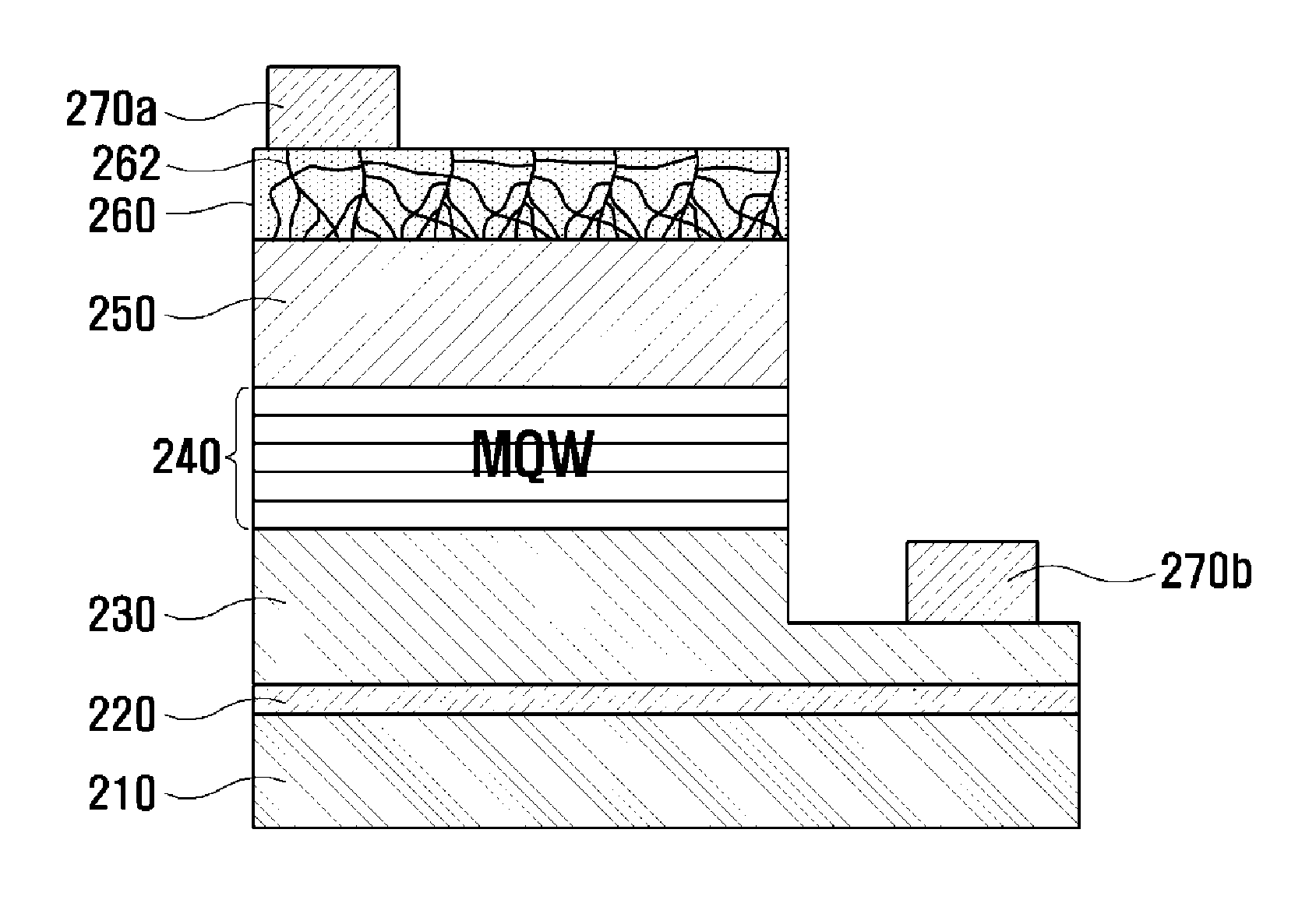
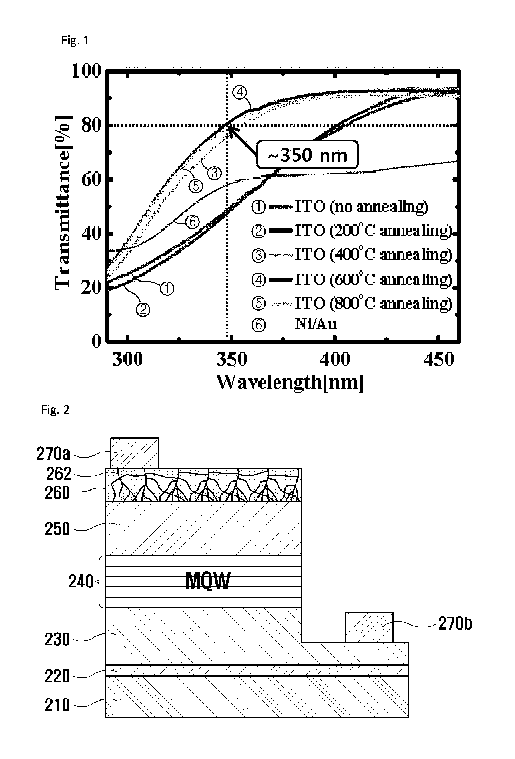
[0048]FIG. 2 is a diagram illustrating a configuration of a light emitting device including a transparent electrode 260 according to the present invention.

[0049]Referring to FIG. 2, the light emitting device according to the first embodiment of the present invention is configured to include, a substrate 210 and a buffer layer 220, a first semiconductor layer 230, an activation layer 240, and a second semiconductor layer 250 which are sequentially formed on the substrate 210. In addition, the light emitting device is configured to include a transparent electrode 260 formed on the second semiconductor layer 250, an electrode pad 270a formed on an upper portion of the transparent electrode 260, and an electrode pad 270b formed on an upper portion of the first semiconductor layer 230 of which a portion region is etched to be exposed.

[0050]The substrate 210 may be constructed by using a substrate such as a sapphire substrate which is generally used for manufacturing a light emitting devi...

second embodiment

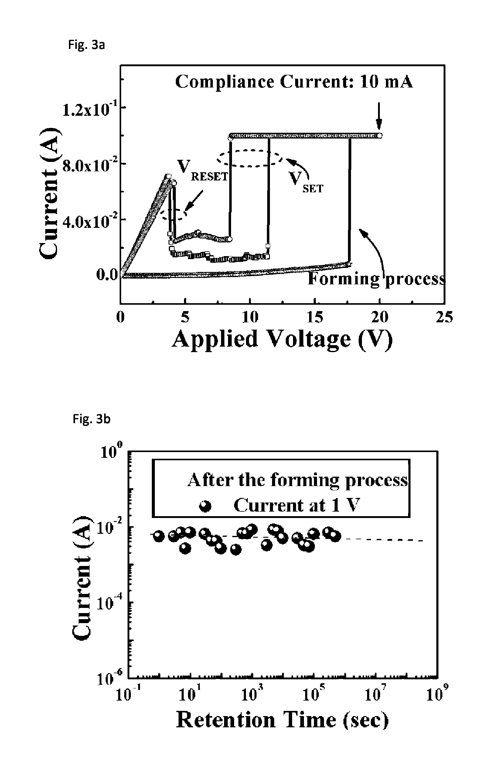
[0076]First, referring to FIG. 6a, the light emitting device according to the present invention has a flip-chip structure where light generated in an activation layer is emitted in the direction of a substrate. The light emitting device is configured by further including a transparent electrode formed by using a resistance change material of the present invention, in which conducting filaments are formed, between a semiconductor layer (p-GaN) and a reflective layer in addition to the light emitting device having a flip-chip structure in the related art.

[0077]In the second embodiment illustrated in FIG. 6a, the surface where a substrate 610 is disposed is referred to as a lower surface. In the same manner as that of the horizontal type light emitting device described with reference to FIGS. 2 to 4, a substrate 610, a buffer layer 620, a first semiconductor layer 630, an activation layer 640, and a second semiconductor layer 650 are sequentially formed, a transparent electrode 660 whe...

third embodiment

[0088]The light emitting device according to the present invention is a vertical type light emitting device. The transparent electrode formed by using a resistance change material in which the conducting filaments are formed is additionally formed between the reflective layer and the second semiconductor layer (for example, p-GaN layer) in a configuration of a general vertical type light emitting device.

[0089]Referring to FIG. 8a, the light emitting device according to the third embodiment of the present invention is configured by sequentially forming a submount substrate 890, an bonding layer 880, a reflective layer 870, a transparent electrode 860, a second semiconductor layer 850, an activation layer 840, a first semiconductor layer 830, and an electrode pad 910.

[0090]In the third embodiment, the submount substrate 890 is constructed with a metal substrate into which current can be injected. The reflective layer 870 is formed on the metal substrate 810 by using a material such as...


PUM


Abstract

Provided are a light emitting device including a transparent electrode having high transmittance with respect to light in a UV wavelength range as well as in a visible wavelength range and good ohmic contact characteristic with respect to a semiconductor layer and a method of manufacturing the light emitting device. A transparent electrode of a light emitting device is formed by using a resistance change material which has high transmittance with respect to light in a UV wavelength range and of which resistance state is to be changed from a high resistance state into a low resistance state due to conducting filaments, which current can flow through, formed in the material if a voltage exceeding a threshold voltage inherent in a material applied to the material, so that it is possible to obtain high transmittance with respect to light in a UV wavelength range.

Description

BACKGROUND OF THE INVENTION[0001]1. Field of the Invention[0002]The present invention relates to a light emitting device including a transparent electrode and a method of manufacturing the light emitting device, and more particularly, to a light emitting device including a transparent electrode having good ohmic contact characteristic and high transmittance and a method of manufacturing the light emitting device.[0003]2. Description of the Related Art[0004]Transparent electrodes have been used in various application fields such as LEDs, solar cells, medical UV sterilizers, and fisheries, and the application fields and their demands have been gradually increased. Particularly, the transparent electrodes have been actively used in the LED field. The transparent electrode technique currently applied to the LEDs is mainly an ITO (indium tin oxide) based technique which can be applied to a visible wavelength range of 400 nm to 800 nm and a UV wavelength range of 365 nm to 400 nm in the e...

Claims


Application Information

Patent Timeline
Patent Type & Authority Patents(United States)
IPC IPC(8): H01L33/60H01L33/32H01L33/42H01L33/06H01L33/00H01L33/40H01L33/14
CPCH01L33/0025H01L33/0075H01L33/0079H01L33/06H01L33/14H01L33/32H01L33/405H01L33/42H01L2933/0016H01L33/36H01L33/46H01L33/62H01L2933/0066H01L33/0093
Inventor KIM, TAE GEUNKIM, HEE-DONG
Owner KOREA UNIV RES & BUSINESS FOUND
Why Eureka
Try Eureka