[0020]A further advantage of the present invention is that an adhesive may be provided which has a high accuracy in nominal thickness and a high uniformity laterally across the sensing chip area. Since it is common that there are strict requirements on the overall accuracy and uniformity of the sensor device, a high accuracy in the thickness of the adhesive allows for a lower planarity of the protective plate, thereby making it possible to maintain overall tolerances with respect to thickness variations while using a less planar / accurate protective plate, which in turns allows the use of a protective plate having a higher surface roughness thereby leading to reduced cost. Moreover, when compared to a molding process, the inventive concept is not relying on accurate placement of the die, nor on back-grinding tolerances of the wafer.
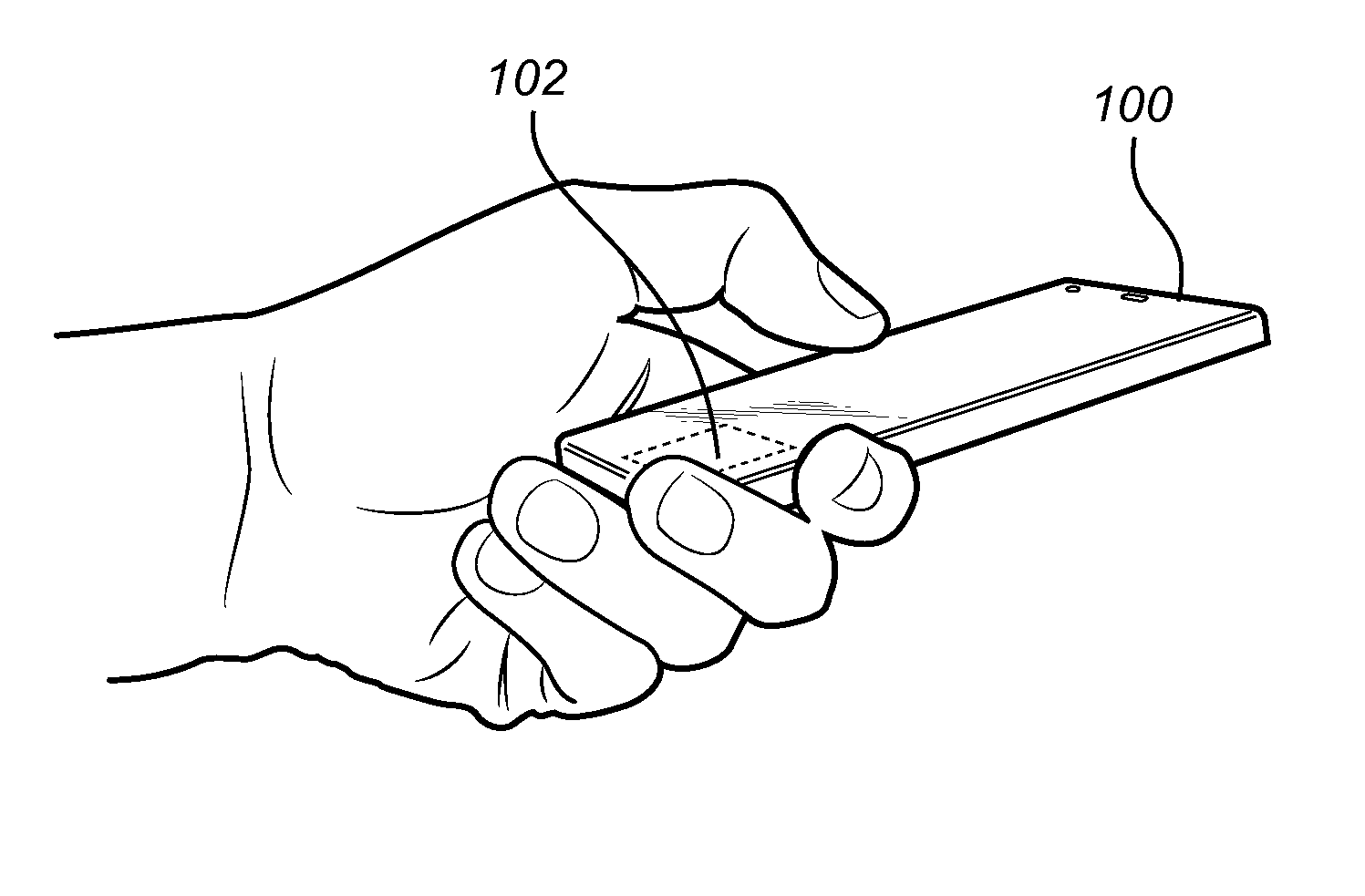
[0021]Moreover, the sensing device according to various embodiments of the invention provides an advantage over alternative solutions for reducing the distance between the sensing element and a finger, such as using an edge trench for arranging the bond pad on the sensing chip. In particular, using an edge trench takes up a certain area outside of the sensing area whereas the sensing device according to the invention offers a higher flexibility in locating the bond pads and thereby provides more efficient area utilization.
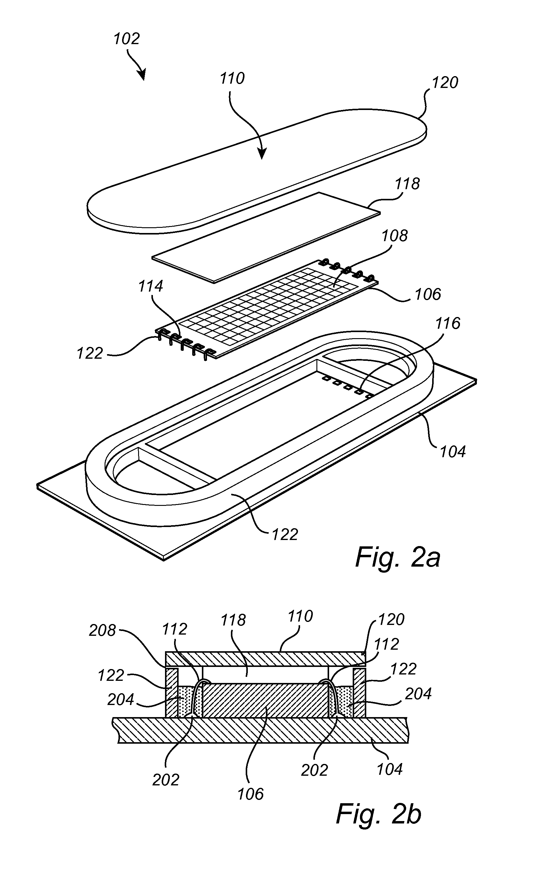
[0022]According to one embodiment of the invention, the adhesive may preferably have a thickness at least equal to the height of the portion of the bond wire protruding above the sensing plane. Since it is desirable to maintain a separation between the protective plate and the bond wire to reduce the risk of disturbances relating to ESD (electrostatic discharge) phenomena, an adhesive thicker than the loop height of the bond wire ensures that there is no contact between the bond wire and the protective plate.
[0023]In one embodiment of the invention, the adhesive may advantageously be an adhesive film comprising a first adhesive layer arranged in contact with the sensing elements, an intermediate carrier layer, and a second adhesive layer arranged in contact with said protective plate. The intermediate carrier layer acts to provide mechanical stability to the adhesive film while still being flexible. Thereby, if the thickness of the first adhesive layer is selected to be lower than the bond wire loop height, the intermediate carrier layer can act to push down on the bond wire when the film is being placed onto the sensing chip so that the wire bond loop height is reduced. This is advantageous since it provides a well defined device where the wire bond loop height is defined by the thickness of the first adhesive layer, the distance between the wire bond and the protective plate is defined by the thickness of the second adhesive layer and the thickness of the intermediate carrier layer, and the distance between the sensing plane and the protective plate is defined by the overall thickness of the tape. The aforementioned adhesive film may also be referred to as a double-sided adhesive film or a double-sided tape. Such double-sided tapes suitable for use in the present application having a high accuracy in thickness and uniformity are commercially available.
[0024]In one embodiment of the invention, the intermediate carrier layer may advantageously comprise a dielectric material. The adhesive is preferably insulating having high electric field breakdown strength. Accordingly, an adhesive having high electric field breakdown strength protects the sensing elements from electrostatic discharge.
[0025]According to one embodiment of the invention, the intermediate carrier layer may advantageously comprise a material having an electric field breakdown strength of at least 100 V / μm, and preferably of at least 200 V / μm. In principle, it is desirable to have an electric field breakdown strength which is as high as possible.

