Organic light emitting display devices and methods of manufacturing organic light emitting display devices

a technology of light-emitting display devices and which is applied in the direction of semiconductor devices, basic electric elements, electrical apparatus, etc., can solve the problems of capacitors not providing sufficient capacitance for other elements of organic light-emitting display devices, and the area of transparent regions may not be sufficiently obtained, so as to achieve the effect of reducing the difference of adjacent refractive indexes, reducing the area of transparent regions, and reducing the transmittan

Active Publication Date: 2017-04-11
SAMSUNG DISPLAY CO LTD
View PDF47 Cites 6 Cited by
  • Summary
  • Abstract
  • Description
  • Claims
  • Application Information

AI Technical Summary

Benefits of technology

[0029]According to example embodiments, the organic light emitting display device may include the substrate, the first transistor, the second transistor, the at least one capacitor, etc. The dielectric structure of the capacitor may include silicon oxynitride. Here, the dielectric constant and the refractive index of the dielectric structure may be adjusted in accordance with the nitrogen content therein, so that the capacitor may provide a sufficient capacitance for elements of the organic light emitting display device. In addition, when the dielectric structure extends from the opaque region to the transparent region, the transmittance of the transparent region may not be substantially reduced because a difference of refractive indices of adjacent layers may be minimized. Furthermore, the additional capacitor may be provided over the capacitor. In other words, the organic light emitting display device may have the configuration in which a plurality of capacitors is substantially vertically stacked. Thus, an area for the capacitors may be substantially reduced compared to the configuration in which the capacitors are disposed in parallel. As a result, the organic light emitting display device may ensure a more sufficient capacitance while increasing an area of the transparent region.

Problems solved by technology

In the conventional transparent organic light emitting display device, since transistors and capacitors are positioned in the opaque region, an area of the transparent region may not be sufficiently obtained, and the capacitor may not provide a sufficient capacitance for other elements of the organic light emitting display device.

Method used


Image

  • Organic light emitting display devices and methods of manufacturing organic light emitting display devices
  • Organic light emitting display devices and methods of manufacturing organic light emitting display devices
  • Organic light emitting display devices and methods of manufacturing organic light emitting display devices

Examples


Embodiment Construction

[0034]Hereinafter, organic light emitting display devices and methods of manufacturing organic light emitting display devices in accordance with example embodiments will be explained in detail with reference to the accompanying drawings.

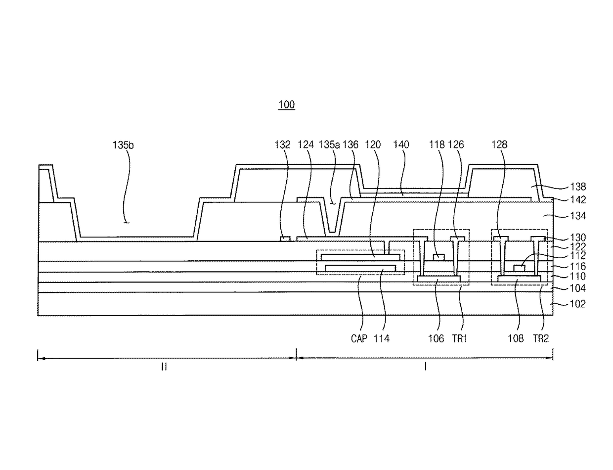
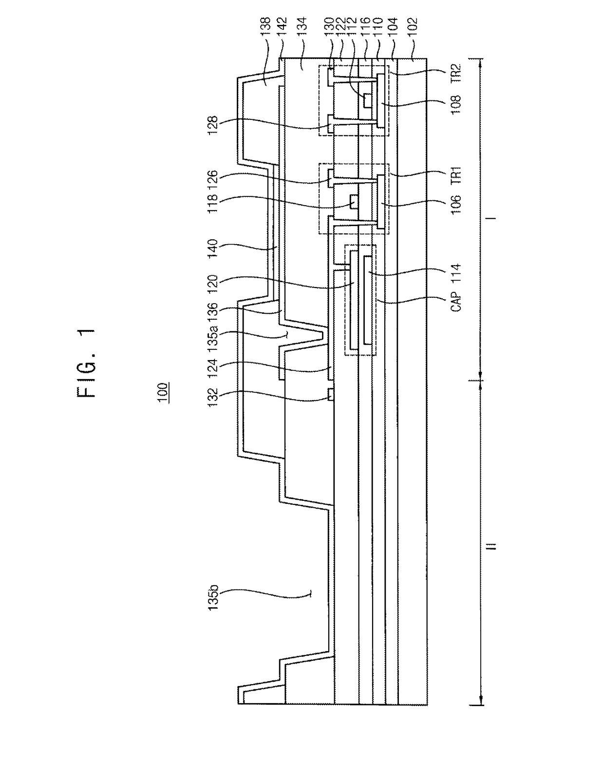
[0035]FIG. 1 is a cross sectional view illustrating an organic light emitting display device 100 in accordance with example embodiments.

[0036]Referring to FIG. 1, the organic light emitting display device 100 may include a substrate 102, a first transistor TR1, a second transistor TR2, a capacitor CAP, an organic light emitting structure 140, etc. The organic light emitting display device 100 may include an opaque region I and a transparent region II. While the organic light emitting display device 100 is in an ON state, an image may be displayed in the opaque region I. Further, while the organic light emitting display device 100 is in an OFF state, an image of an object positioned before and / or after the transparent region II of the organic light em...


PUM


Abstract

An organic light emitting display device includes a substrate, a first transistor disposed on the substrate in the opaque region, a second transistor disposed on the substrate in the opaque region, the second transistor being adjacent to the first transistor along a first direction, and a capacitor disposed on the substrate in the opaque region, the capacitor being adjacent to the first transistor along a second direction different from the first direction. Here, the capacitor may include a first capacitor electrode, a dielectric structure including silicon oxynitride and a second capacitor electrode.

Description

CROSS-REFERENCE TO RELATED APPLICATION(S)[0001]This application claims priority under 35 U.S.C. §119 to Korean patent Application No. 10-2014-0090714, filed on Jul. 18, 2014, the disclosure of which is hereby incorporated by reference herein in its entirety.BACKGROUND[0002]1. Technical Field[0003]Example embodiments relate to organic light emitting display devices and methods of manufacturing organic light emitting display devices. More particularly, example embodiments relate to organic light emitting display devices including at least one capacitor having a dielectric structure containing silicon oxynitride, and methods of manufacturing the organic light emitting display devices.[0004]2. Description of the Related Art[0005]Recently, a transparent organic light emitting display device has been rapidly developed. The transparent organic light emitting display device may include a transparent region and an opaque region. In the transparent organic light emitting display device, an im...

Claims


Application Information

Patent Timeline
Patent Type & Authority Patents(United States)
IPC IPC(8): H01L27/32H01L21/02H01L27/12H01L29/49H01L29/51H01L49/02H01L51/56
CPCH01L29/518H01L27/1259H01L27/326H01L27/3262H01L27/3265H01L29/4908H01L27/3258H01L27/1237H01L27/1255H10K59/121H10K59/1216H10K59/124H10K59/1213
Inventor PARK, SANG-HOJANG, JAE-HYUKKIM, CHANG-OKYOON, JOO-SUNJANG, YONG-JAE
Owner SAMSUNG DISPLAY CO LTD
Why Eureka
Try Eureka