Array substrate and manufacturing method thereof, as well as display device

a technology of array substrate and manufacturing method, applied in the field of array substrate, can solve the problem of relatively low transmittance at the edge of the pixel, and achieve the effect of improving the display effect, and increasing the transmittance at the edge of the pixel

Active Publication Date: 2017-04-25
BOE TECH GRP CO LTD +1
View PDF13 Cites 0 Cited by
  • Summary
  • Abstract
  • Description
  • Claims
  • Application Information

AI Technical Summary

Benefits of technology

[0005]Embodiments of the present invention provide an array substrate and a manufacturing method thereof, as well as a display device, which can increase transmittance at the edge of a pixel, thereby improving a display effect.
[0017]In the array substrate and the manufacturing method thereof as well as the display device provided by the embodiments of the present invention, an auxiliary common electrode is additionally arranged between the adjacent pixel electrodes, and the auxiliary common electrode is electrically connected with the common electrode. In this way, in addition to the electric field formed between the pixel electrodes and the common electrode, the pixel electrodes can also form an additional auxiliary electric field with the auxiliary common electrode so as to drive the liquid crystal molecules at the edge of a pixel, so, the driving electric field at the edge of the pixel will be strengthened, so that the liquid crystal molecules will be deflected more sufficiently, and the transmittance will be higher. Therefore, the technical solutions of the embodiments of the present invention can increase the transmittance at the edge of the pixel, and improve the display effect.

Problems solved by technology

However, for a display device in the FFS display mode, the driving electric field at the edge of each pixel is much weaker than the driving electric field within the pixel, such that the liquid crystals are hardly deflected, so the light transmittance at the edge of the pixel is relatively low, which influences a display effect.

Method used


Image

  • Array substrate and manufacturing method thereof, as well as display device
  • Array substrate and manufacturing method thereof, as well as display device
  • Array substrate and manufacturing method thereof, as well as display device

Examples


Embodiment Construction

[0026]Next, the technical solutions in the embodiments of the present invention will be described clearly and completely in combination with drawings in the embodiments of the present invention. The embodiments described are only part of rather than all of the embodiments of the present invention.

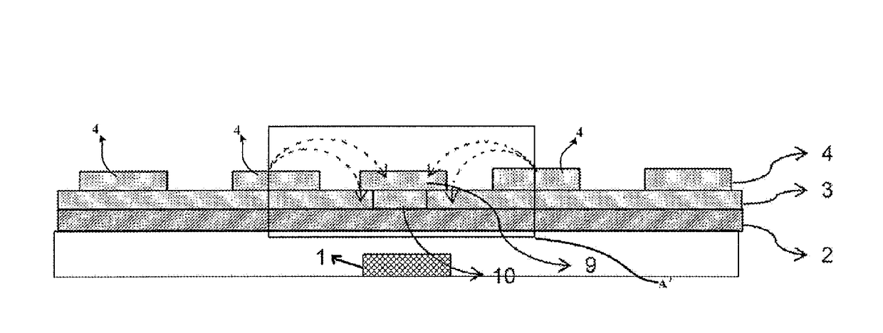
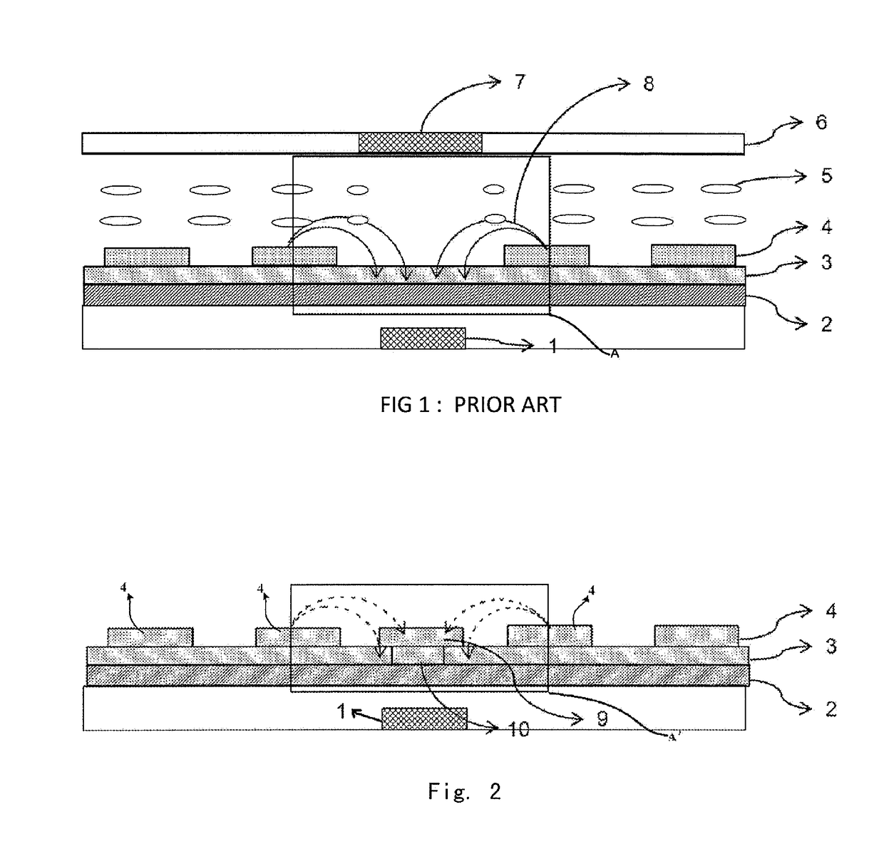
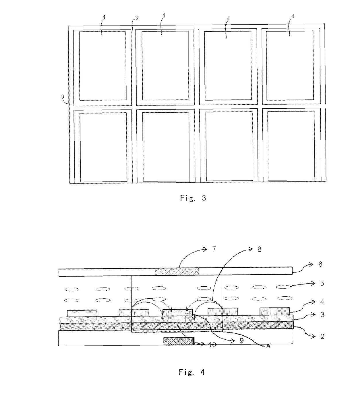
[0027]An embodiment of the present invention provides an array substrate, as shown in FIG. 2. The array substrate comprises: a common electrode 2 and pixel electrodes 4. In addition to this, the array substrate further comprises an auxiliary common electrode 9 arranged between adjacent pixel electrodes 4 and electrically connected with the common electrode 2. Specifically, the number of the pixel electrodes 4 is multiple.

[0028]The array substrate provided by the embodiment of the present invention is adapted for use in a display device in a plane field mode, such as a display device in a FFS, an IPS (In Plane Switching), or an ADS (Advanced-Super Dimensional Switching) mode. An auxiliary co...


PUM

PropertyMeasurementUnit
transmittanceaaaaaaaaaa
coloraaaaaaaaaa

Abstract

Embodiments of the present invention disclose an array substrate and a manufacturing method thereof, as well as a display device, which relates to the field of display, and can increase transmittance at the edge of a pixel, thereby improving display effect. The array substrate provided by the present invention comprises: a common electrode and pixel electrodes, the array substrate further comprises an auxiliary common electrode arranged between adjacent pixel electrodes and electrically connected with the common electrode.

Description

RELATED APPLICATIONS[0001]This application is the U.S. national stage entry of PCT / CN2015 / 074284, filed Mar. 16, 2015, which claims priority to Chinese Application No. 201410592074.9, filed Oct. 29, 2014, the entire disclosures of which are incorporated by reference herein.FIELD OF THE INVENTION[0002]The present invention relates to the field of display, particularly to an array substrate and a manufacturing method thereof, as well as a display device.BACKGROUND OF THE INVENTION[0003]The Fringe Field Switching (FFS) display mode is one of plane field modes, which has advantages of high transmittance and clear images.[0004]FIG. 1 is a structural schematic view of a display device in a FFS mode. An insulating layer is formed after a data line 1 of an array substrate is formed, a common electrode 2 is formed on the insulating layer, then another insulating layer 3 is formed, and pixel electrodes 4 are formed on the insulating layer 3. For a color film substrate arranged opposite to the...

Claims


Application Information

Patent Timeline
Patent Type & Authority Patents(United States)
IPC IPC(8): G02F1/1343G02F1/1362H01L27/12G02F1/1333H01L21/77
CPCG02F1/134309G02F1/13439G02F1/133345G02F1/136286H01L21/77H01L27/12H01L27/124H01L27/1262G02F2001/134318G02F2001/134372G02F2201/121G02F2201/123G02F1/134372G02F1/134318
Inventor WANG, ZHENWEIWANG, KAIXUANFANG, YEZHOUZHU, HONGYU, HONGJUN
Owner BOE TECH GRP CO LTD
Why Eureka
Try Eureka