Semiconductor device and manufacturing method thereof

a technology of semiconductor devices and manufacturing methods, applied in semiconductor devices, semiconductor/solid-state device details, electrical devices, etc., can solve problems such as difficult to adjust the depth of contact holes, process defects may occur, and use a complicated manufacturing process

Active Publication Date: 2017-04-25
SK HYNIX INC
View PDF5 Cites 21 Cited by
  • Summary
  • Abstract
  • Description
  • Claims
  • Application Information

AI Technical Summary

Benefits of technology

[0008]Embodiments provide a semiconductor device and a manufacturing method thereof, which can reduce the occurrence of defects when contact plugs of the semiconductor device are formed.
[0012]According to embodiments of the present invention, an interlayer insulating layer is formed on conductive layers and insulating layers which are alternately stacked in a step shape, and the lengths of contact plugs connected to the conductive layers by penetrating a subsequent interlayer insulating layer are formed to be uniform by patterning the interlayer insulating layer in a step shape. Thus, it is possible to prevent a contact bridge phenomenon and a contact failure between the contact plug and the conductive layer.

Problems solved by technology

However, to implement such a structure, contact plugs having various depths should be formed which results in using a complicated manufacturing process.
For example, in a process of forming a contact plug, it is difficult to adjust the depth of a contact hole due to a step difference of an Interlayer insulating layer.
Therefore, the contact plug may penetrate a word line, thereby causing a bridge.
Alternatively, the contact plug may not reach the word line, and therefore, a process defect may occur.

Method used


Image

  • Semiconductor device and manufacturing method thereof
  • Semiconductor device and manufacturing method thereof
  • Semiconductor device and manufacturing method thereof

Examples


Embodiment Construction

[0020]In the following detailed description, only certain exemplary embodiments of the present invention have been shown and described by way of illustration. As those skilled in the art would realize, the described embodiments may be modified in various different ways, all without departing from the spirit or scope of the present invention. Accordingly, the drawings and description are to be regarded as illustrative in nature and not restrictive.

[0021]In the entire specification, when an element is referred to as being “connected” or “coupled” to another element, it can be directly connected or coupled to another element or be indirectly connected or coupled to another element with one or more intervening elements interposed therebetween. In addition, when an element is referred to as “including” a component, this indicates that the element may further include another component instead of excluding another component unless there is a different disclosure.

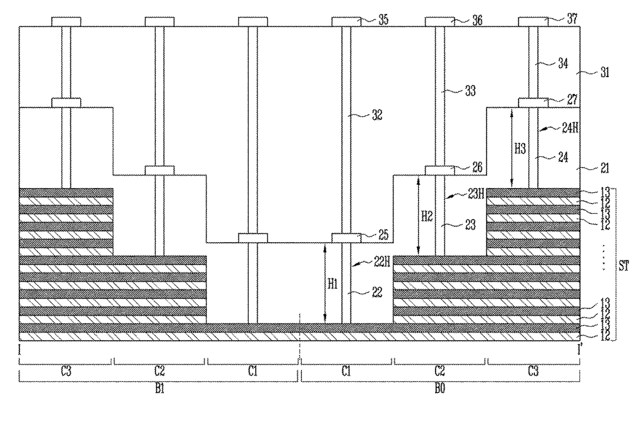
[0022]FIG. 1 is a perspecti...


PUM


Abstract

A semiconductor device and a manufacturing method thereof are provided. A semiconductor device includes a stack structure including conductive layers stacked in a step shape, a first interlayer insulating layer formed over the stack structure, the first interlayer insulating layer including contact holes with a uniform depth, which expose the conductive layers, lower contact plugs formed in the contact holes, the lower contact plugs being respectively contacted with the conductive layers, and lower contact pads respectively connected to the contact plugs.

Description

CROSS-REFERENCE TO RELATED APPLICATION[0001]The present application claims priority to Korean patent application number 10-2015-0059978, filed on Apr. 28, 2015, the entire disclosure of which is herein incorporated by reference in its entirety.BACKGROUND[0002]1. Field[0003]An aspect of the present invention relates to a semiconductor device and a manufacturing method thereof, and more particularly, to a semiconductor device having a three-dimensional structure and a manufacturing method thereof.[0004]2. Discussion of Related Art[0005]A nonvolatile memory device is a memory device in which stored data are maintained when a power supply is interrupted. As integration of a two-dimensional memory device in which memory cells are formed in a single layer on a silicon substrate reaches its limits, there has recently been proposed a three-dimensional nonvolatile memory device in which memory cells are vertically stacked on a silicon substrate.[0006]The three-dimensional nonvolatile memory ...

Claims


Application Information

Patent Timeline
Patent Type & Authority Patents(United States)
IPC IPC(8): H01L23/00H01L23/528H01L23/522H01L23/535H01L21/768H01L27/11556H01L27/11548H01L27/11575H01L27/11582
CPCH01L23/528H01L21/76816H01L21/76877H01L21/76895H01L23/5226H01L23/535H01L27/11548H01L27/11556H01L27/11575H01L27/11582H10B41/50H10B41/27H10B43/50H10B43/27
Inventor KIM, HAE SOO
Owner SK HYNIX INC
Why Eureka
Try Eureka