Memory-testing device and memory-testing method

a memory test and memory technology, applied in the direction of static storage, instruments, etc., can solve the problems of large size of the test pattern of atpg, failure of memory output, and deterioration of test reliability and accuracy of the test circuitry b>120/b>, so as to reduce the timing slack of the memory test device

Active Publication Date: 2017-05-16
MEDIATEK INC
View PDF5 Cites 0 Cited by
  • Summary
  • Abstract
  • Description
  • Claims
  • Application Information

AI Technical Summary

Benefits of technology

[0008]In an embodiment of the present invention, a memory-testing device for testing a memory is provided. The memory-testing device includes a testing circuitry and a register. The testing circuitry is coupled to the memory for testing the performance of the memory. The register is coupled to the testing circuitry and input by a testing clock signal, wherein the testing clock signal is different from the original clock signal of the memory and / or the testing circuitry. The testing clock signal is utilized for adjusting the time when the memory-testing device latches data from the memory to decrease the timing slack of the memory-testing device.
[0009]In an embodiment of the present invention, a memory-testing method for testing a memory is provided. The memory-testing method includes generating a testing clock signal of a register wherein the testing clock signal is different from an original clock signal of the memory and / or a testing circuitry utilized for testing performance of the memory; and adjusting the time when the memory-testing device latches data from the memory by the testing clock signal to decrease a timing slack of the memory-testing device.

Problems solved by technology

However, if the timing margin of the third timing path TP3 is larger than or looser than the second timing path TP2, the testing reliability and the accuracy of the testing circuitry 120 will deteriorate.
Since the critical path is from the pre-charging of the bit line to the next access cycle, there could be some failures in the output DO of the memory 160 if the critical path is too tight to pre-charge the bit line to a pre-determined voltage level.
In addition, the size of the test pattern of the ATPG is very large.
Therefore, the testing procedure of ATPG is inefficient and also costs too much time and money, and another memory-testing method with high efficiency and low cost is needed.

Method used


Image

  • Memory-testing device and memory-testing method
  • Memory-testing device and memory-testing method
  • Memory-testing device and memory-testing method

Examples


Embodiment Construction

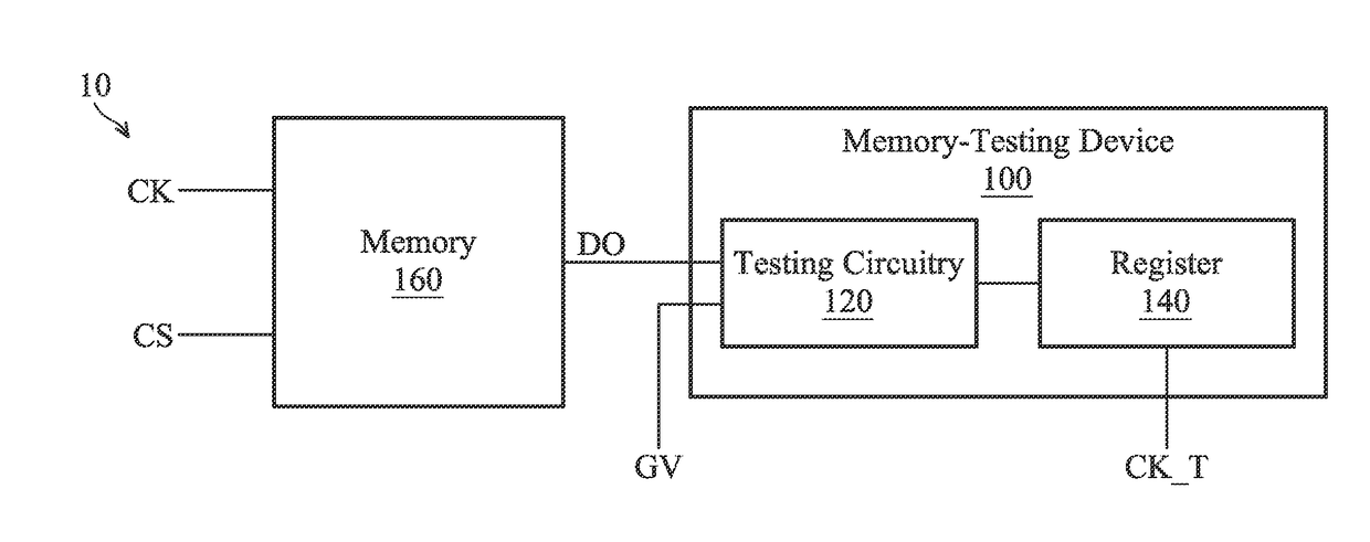
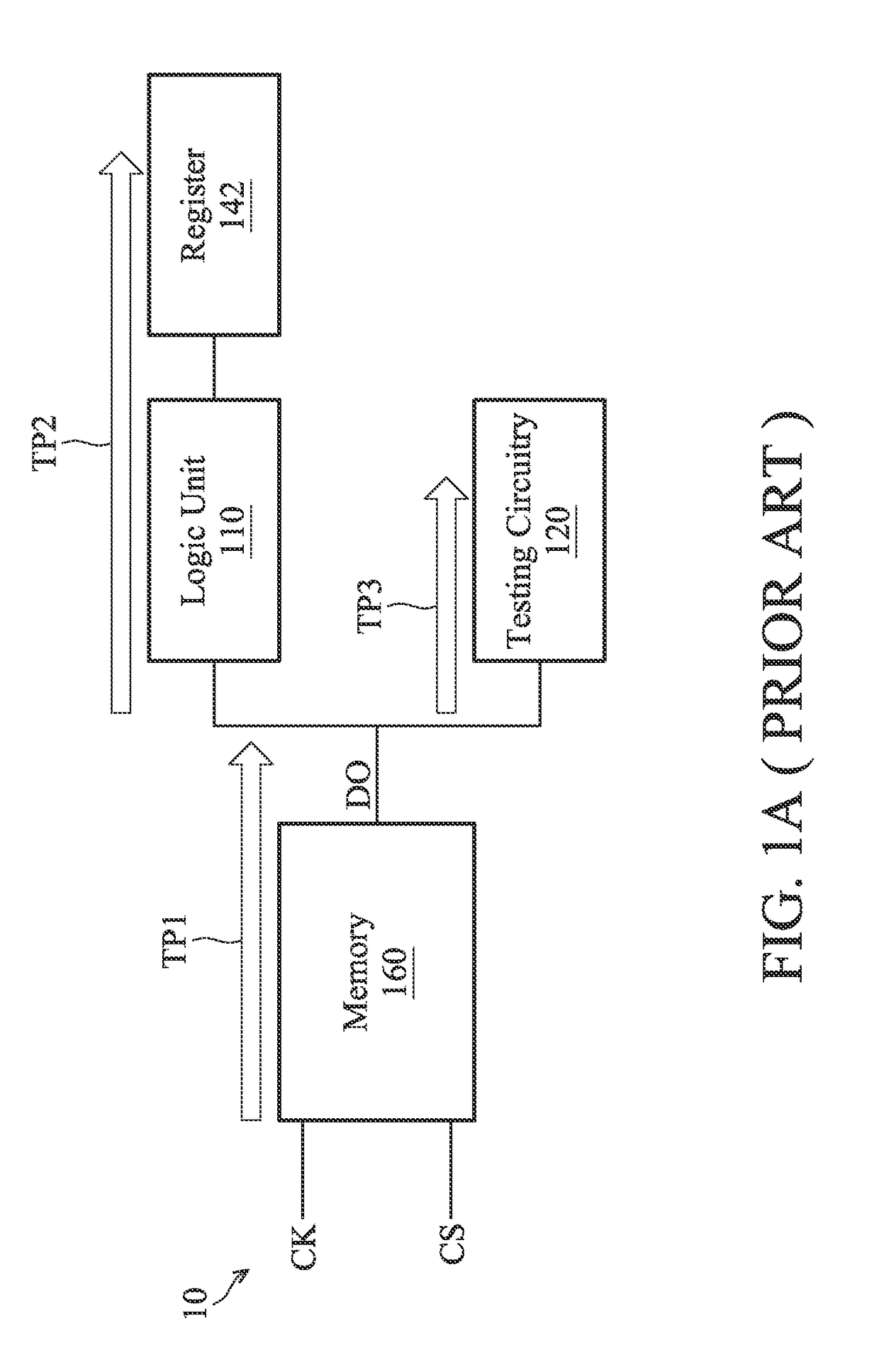
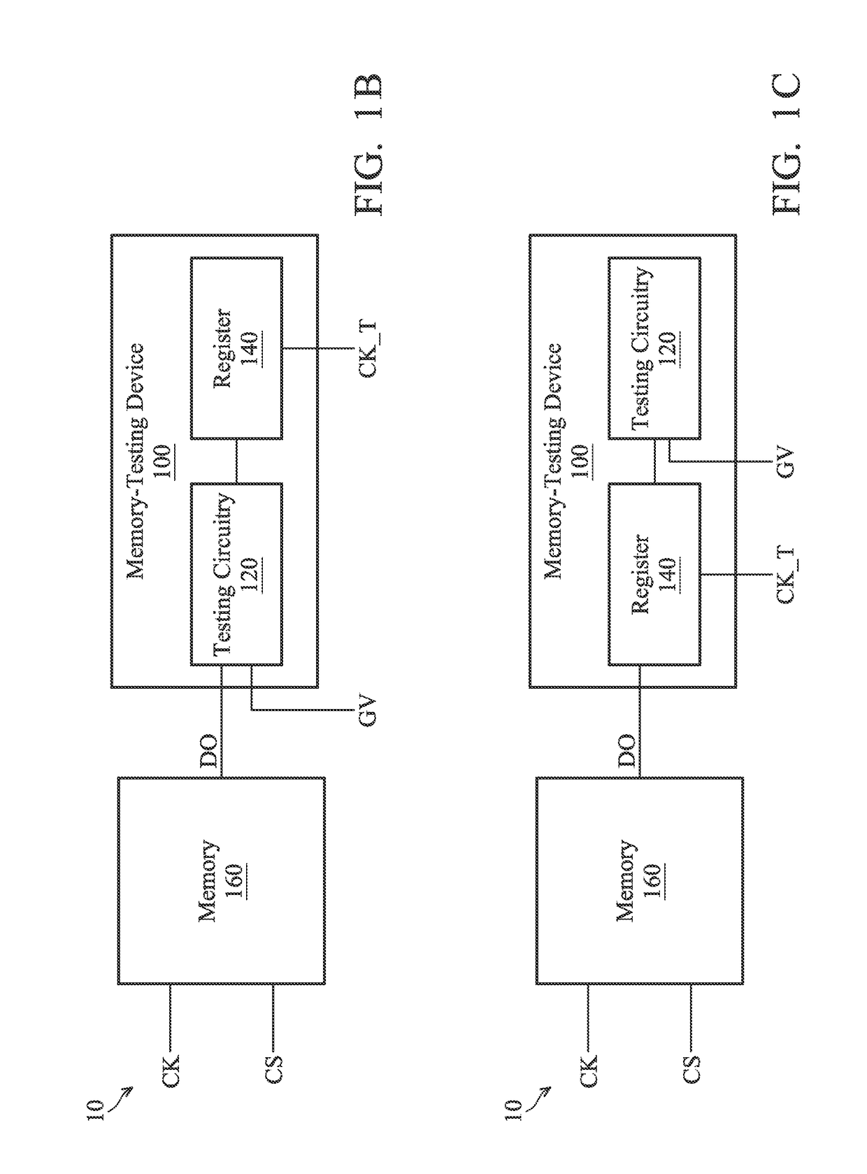
[0027]The following description is of the best-contemplated operation of carrying out the invention. This description is made for the purpose of illustrating the general principles of the invention and should not be taken in a limiting sense. Certain terms and figures are used throughout the description and following claims to refer to particular components. As one skilled in the art will appreciate, manufacturers may refer to a component by different names. This document does not intend to distinguish between components that differ in name but not function. The terms “component”, “system” and “device” used in the present invention could be the entity relating to the computer which is hardware, software, or a combination of hardware and software. In the following description and in the claims, the terms “include” and “comprise” are used in an open-ended fashion, and thus should be interpreted to mean “include, but not limited to . . . ”. Also, the term “couple” is intended to mean e...


PUM


Abstract

A memory-testing device for testing a memory is provided. The memory-testing device includes a testing circuitry and a register. The testing circuitry is coupled to the memory for testing performance of the memory. The register is coupled to the testing circuitry and inputted by a testing clock signal, wherein the testing clock signal is different from an original clock signal of the memory and / or the testing circuitry. The testing clock signal is utilized for adjusting the time when the memory-testing device latches data from the memory to decrease a timing slack of the memory-testing device.

Description

CROSS REFERENCE TO RELATED APPLICATIONS[0001]This application claims the benefit of U.S. Provisional Application No. 61 / 938,961, filed on Feb. 12, 2014, the entirety of which is / are incorporated by reference herein.BACKGROUND OF THE INVENTION[0002]Field of the Invention[0003]This disclosure relates generally to a memory-testing device and, more particularly, to an effective memory-testing method with an adjustable clock signal to optimize the timing slack of the memory-testing device.[0004]Description of the Related Art[0005]FIG. 1A is a block diagram of a system 10 including a memory 160 operated in a functional mode or a test mode. The system 10 includes a logic unit 110, testing circuitry 120, a register 142 and a memory 160. There are several timing paths for accessing the memory 160 including a first timing path TP1 from the original clock signal CK of the memory 160 to the output DO of the memory 160, a second timing path TP2 from the output DO of the memory 160 through the lo...

Claims


Application Information

Patent Timeline
Patent Type & Authority Patents(United States)
IPC IPC(8): G11C29/00G11C29/56G11C29/12
CPCG11C29/56012G11C29/12015
Inventor SU, CHIN-JUNGHUANG, REI-FU
Owner MEDIATEK INC
Why Eureka
Try Eureka