Micromechanical device with an actively deflectable element

a micromechanical and active technology, applied in the direction of microelectromechanical systems, semiconductor devices, electromechanical/electrostrictive/magnetostrictive devices, etc., can solve the problems of slow response, further problems, and restricted material set, so as to achieve tremendous relief of manufacturing.

Active Publication Date: 2017-06-13
FRAUNHOFER GESELLSCHAFT ZUR FOERDERUNG DER ANGEWANDTEN FORSCHUNG EV
View PDF12 Cites 3 Cited by
  • Summary
  • Abstract
  • Description
  • Claims
  • Application Information

AI Technical Summary

Benefits of technology

[0010]In accordance with a first aspect of the present application, a micromechanical element with an actively deflectable element is implemented using a layer stack which, upon application of attractive forces between the layers, provokes the deflection. In accordance with the first aspect, however, the attractive force is turned into a deflection of the beam directly rather than via a detour according to which the attractive forces are firstly turned into lateral stresses developing in the layers which, by offsetting the layers relative to a neutral axis of the deflectable element, deflect the deflectable element. In particular, to this end, spacers between the layers are inclined relative to a layer stack direction. Attractive forces between the layers bend the spacers thereby resulting in two opposed stress gradients manifesting themselves at the interfaces between spacers and layers all along the lateral direction with these opposed stress gradients finally bending the deflectable element. Owing to the fact that the lever arm in form of a distance from a neutral axis is not necessary, the stiffness of the deflectable element may be selected more freely.
[0011]In accordance with a second aspect of the present application, the concept of using a laminar actuator of a deflectable element of a micromechanical device, the layer stack being arranged offset to a neutral axis of the deflectable element so as to deflect the deflectable element by exposing the layer stack to an attractive force between its proximal and distal layers, is rendered more effective in terms of achievable deflection amount at a certain attractive force being applied between the layers, by forming each segment into which the layer stack is segmented along a lateral direction in a predetermined way. In particular, in each segment, a surface of the proximal layer which faces the distal layer by a gap between proximal and distal layer, bulges out towards or away from the neutral axis, wherein a ratio of half a length of the respective segment in the lateral direction to a difference between a maximum distance of said surface from the neutral axis and a minimum distance of said surface from the neutral axis lies between sin(1°) and sin(10°), both inclusively. Choosing “slope angle” for each bulge / segment results in an effective exploitation of the deflection of the deflective element responsive to the attractive forces between proximal and distal layers.
[0012]In accordance with a third aspect of the present application, the concept of using a laminar actuator of a deflectable element of a micromechanical device, a laminar actuator being arranged offset from the neutral axis of the deflectable element so as to deflect the deflectable element responsive to an exposure of the layer stack to an attractive force between its proximal and distal layers, is rendered more effective in terms of deflection amount responsive to the exposure to an attractive force between proximal and distal layers by forming, in each segment, the gap between the proximal and distal layer in a non-planar manner and providing the deflectable element's surface facing away from the gap with a shape conforming to the gap. This “conformity” turns out to maintain the stiffness of the deflectable element on the one hand, but increase the achievable deflection amount upon application of a predetermined attractive force between proximal and distal layers on the other hand.
[0014]In accordance with an embodiment associated with a first aspect, each spacer may be formed of insulating material for isolating the layers from one another, wherein each spacer also be formed of a conductive material of the distal and proximal layers, wherein the conductive material extends up into the spacers so as to abut, within the spacers, on the insulating material along a surface which, when exposing the layer stack to attractive force, crosses a tensile stress field developing in the spacers due to the attractive force perpendicularly and is in parallel to a compressive stress of a compression field in the spacers developing in the spacers due to the attractive force. Choosing the interface between both materials along the just outlined surface increases the mechanical stability of the contact between the layers and the spacer.
[0015]In accordance with an embodiment associated with a first aspect, the conductive material of the layers may be interdigitated with insulating material of the spacers at ends of the spacers facing the distal and proximal layers, respectively, i.e., at the interfaces therebetween. Thereby, the delamination probability is reduced.
[0017]The bulging-out of the gap of the segments in accordance with the second aspect may be such that the distal layer's surface facing the neutral axis bulges-out in a rounded, angled or stepped manner. In accordance with embodiments associated with the second aspect, the gap between the proximal layer and the distal layer—or the interface between the gap and the distal layer—may be formed of plane portions and ramp portions exclusively, with the plane portions extending in parallel to the neutral axis and the ramp portions being inclined relative to the neutral axis. Advantageously, the angle of inclination of the ramp portions may be chosen so as to coincide with angles between crystal planes of the material of the deflectable element. By this measure, the manufacturing may be alleviated tremendously.

Problems solved by technology

This causes even further problems.
Disadvantageously, however, the response is slow and high temperature differences may be used in order to achieve high deflections.
Beyond this, the set of suitable materials is restricted.
Here, dealing with the useful materials causes a problem since these materials hinder the usage of usual semiconductor fabrication processes.
All in all, the production of such actuating structures is expensive.
Unfortunately, even the manufacturing of micromechanical devices using the just outlined electrostatic bimorph actuator is demanding.

Method used


Image

  • Micromechanical device with an actively deflectable element
  • Micromechanical device with an actively deflectable element
  • Micromechanical device with an actively deflectable element

Examples


Embodiment Construction

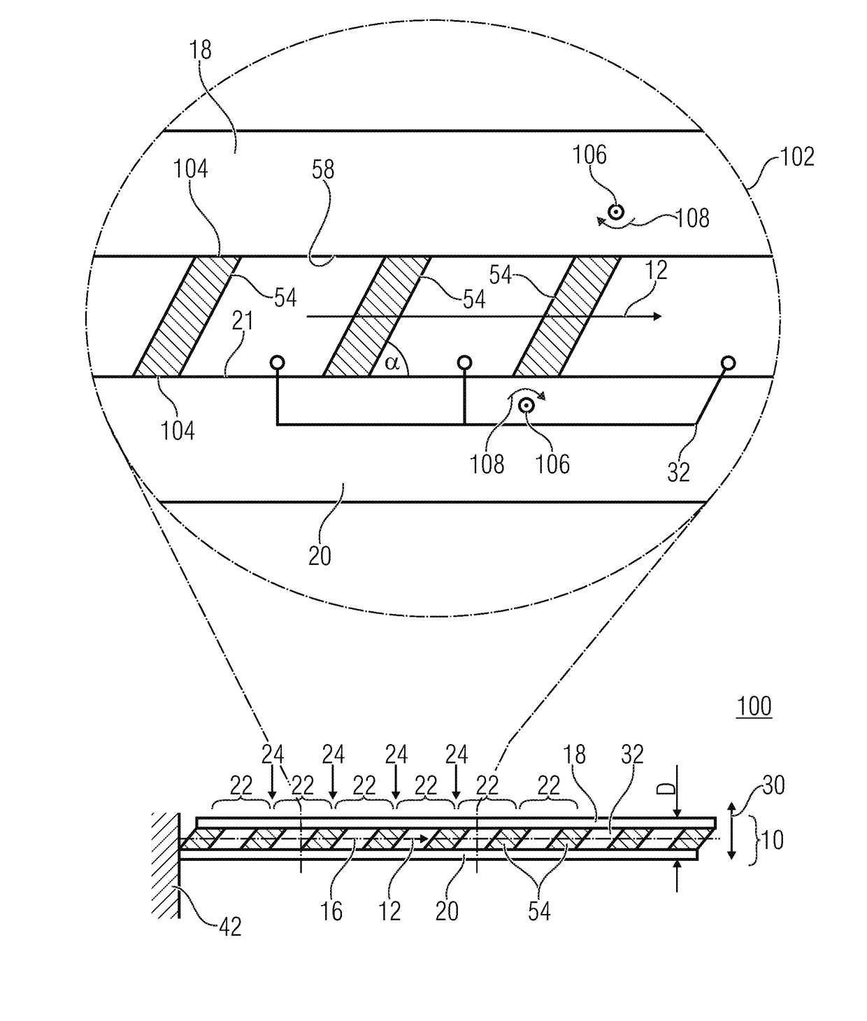
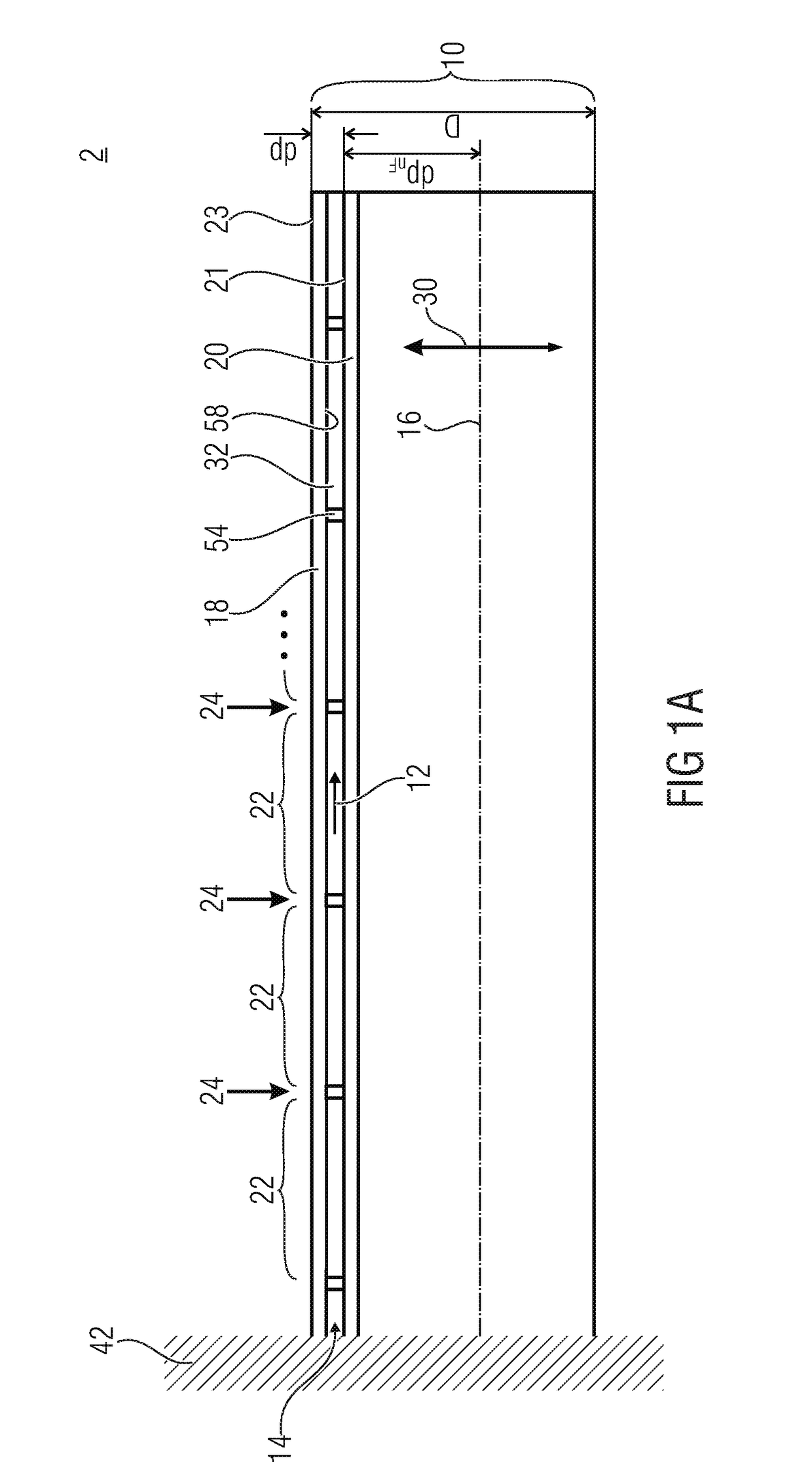
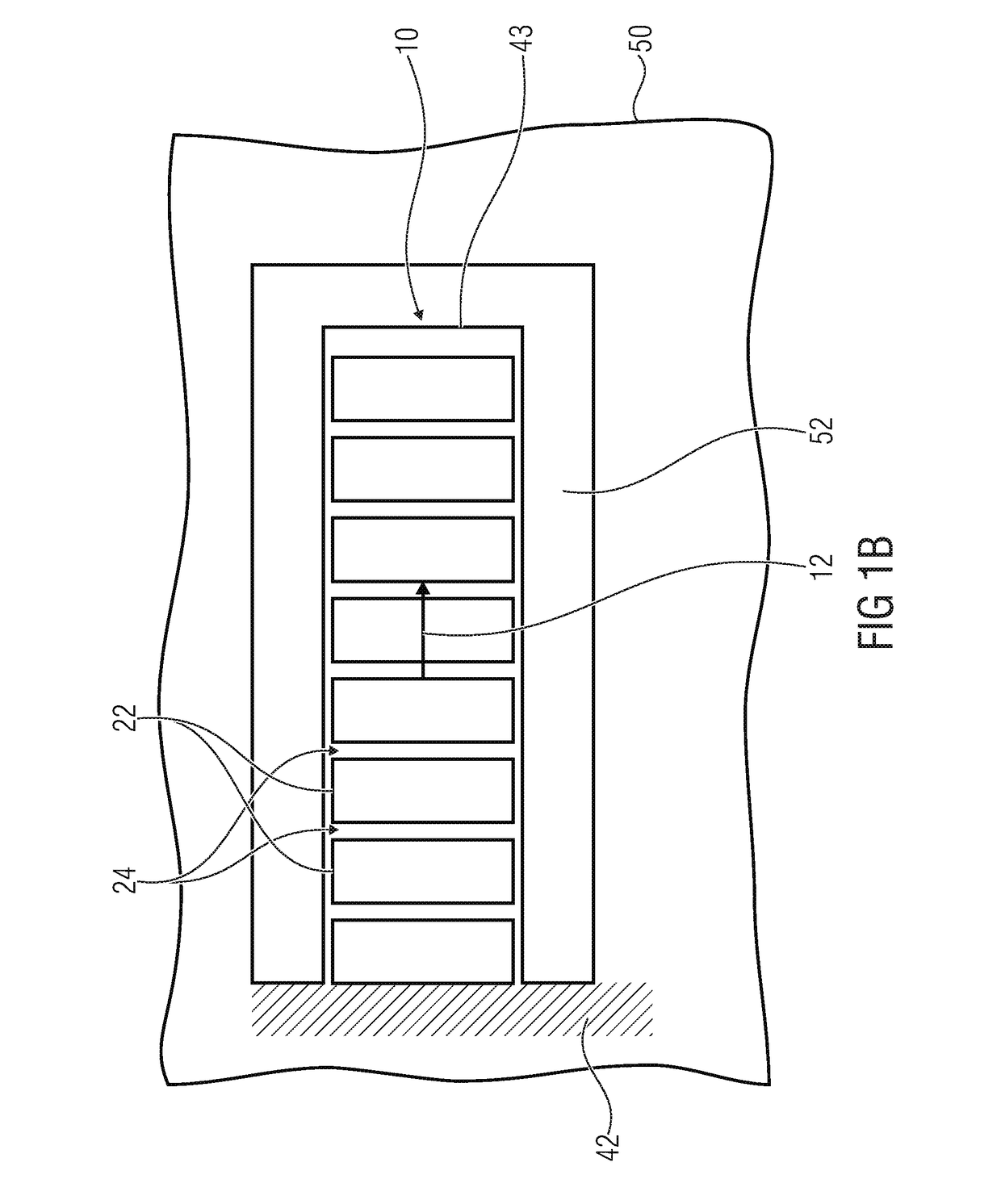
[0051]Before starting with the description of embodiments of the present application in accordance with various aspects of the present application, comparison embodiments of micromechanical devices are described so as to form a reservoir of possible variations in implementing the layer stack which is commonly used in accordance with the subsequently explained embodiments of the various aspects. It is to emphasized, however, that the deflection principle on which these comparison embodiments are based, differs from the principle being the subject of embodiments of the first aspect. Nevertheless, the structural variations of the comparison embodiments as far as the layer stack and the spacers and the gap therebetween is concerned shall be applicable so as to vary embodiments described later with respect to the first aspect, irrespective of the other elements shown in these figures and not occurring in the first aspect's embodiments. With respect to the embodiments of the second and th...


PUM


Abstract

Micromechanical devices include actively deflectable elements. The activation is performed by a layer stack which causes the deflection responsive to attractive forces acting upon the layers of the layer stack.

Description

CROSS-REFERENCE TO RELATED APPLICATIONS[0001]This application claims priority from German Patent Application No. 102015206774.2, which was filed on Apr. 15, 2015, and is incorporated herein in its entirety by reference.[0002]The present invention is concerned with a micromechanical device comprising an actively deflectable element.BACKGROUND OF THE INVENTION[0003]Micromechanical devices having a deflectable element such as a cantilever or membrane are used in a multitude of technical fields, such as in spatial light modulators or in projectors for beam deflection, just to mention a few examples.[0004]Primarily, electrostatic attraction used in micro and nano actuators as the principle for deflection. Mostly, different electrostatic potentials are applied to a deflectable element and a static electrode so that by aid of an electrostatic attraction developing therebetween, a deflection is caused. The force is indirectionally proportional to the square of the distance between the defle...

Claims


Application Information

Patent Timeline
Patent Type & Authority Patents(United States)
IPC IPC(8): H01L29/84B81B3/00
CPCB81B3/0021B81B2201/032B81B2203/0118B81B2203/0127B81B3/0094
Inventor GAUDET, MATTHIEUSCHIMMANZ, KLAUSSTOLZ, MICHAELLANGA, SERGIUCONRAD, HOLGERKAISER, BERT
Owner FRAUNHOFER GESELLSCHAFT ZUR FOERDERUNG DER ANGEWANDTEN FORSCHUNG EV
Why Eureka
Try Eureka