White organic light emitting device

a light-emitting device and organic technology, applied in the direction of semiconductor devices, basic electric elements, electrical appliances, etc., can solve the problems of limited emission characteristic and lifetime, inability to show sufficient luminance of blue emission layer formed of fluorescence material in comparison with phosphorescence material, incomplete transfer of energy, etc., to achieve the effect of enhancing emission efficiency and lifetim

Active Publication Date: 2017-06-20
LG DISPLAY CO LTD
View PDF22 Cites 5 Cited by
  • Summary
  • Abstract
  • Description
  • Claims
  • Application Information

AI Technical Summary

Benefits of technology

[0010]In a related art organic light emitting device, emission characteristic and a lifetime are limited due to an emission structure and a material of an organic emission layer. Therefore, various methods for enhancing emission efficiency and a lifetime are proposed.

Problems solved by technology

For this reason, the blue emission layer formed of a fluorescence material cannot show sufficient luminance in comparison with a phosphorescence material.
In a related art organic light emitting device, emission characteristic and a lifetime are limited due to an emission structure and a material of an organic emission layer.
However, it is incomplete to transfer energy to a dopant, and it is difficult to adjust a balance of white color.
Moreover, a component of a dopant included in a corresponding emission layer is limited due to a characteristic of a dopant itself.
For this reason, a color range capable of expression is narrowed, and consequently, it is difficult to realize a desired color reproduction rate.
However, there is a limitation in adjusting a component or an amount of a dopant included in each of emission layers for improving characteristics of the emission layers.
However, when the emission layers or the organic layers are thickly formed, the number of processes increases, and a lifetime is shortened.
For this reason, it is difficult to apply an organic light emitting device to an organic light emitting device having a large area.
Also, organic layers configuring an emission part may include a plurality of layers having a movement characteristic of an electron or a hole, but in this case, the thickness of the device is thickened, causing an increase in the driving voltage of the device.
Also, since the thicknesses or number of the organic emission layers affect emission efficiency or emission intensity, the inventors have recognized that it is very difficult to set a desired number or thickness.
Therefore, the inventors have recognized that it is very difficult to configure a device with an organic layer having a desired characteristic and a desired number or thickness without any increase in a thickness and manufacture a device for realizing desired white color.

Method used


Image

  • White organic light emitting device
  • White organic light emitting device
  • White organic light emitting device

Examples


first embodiment

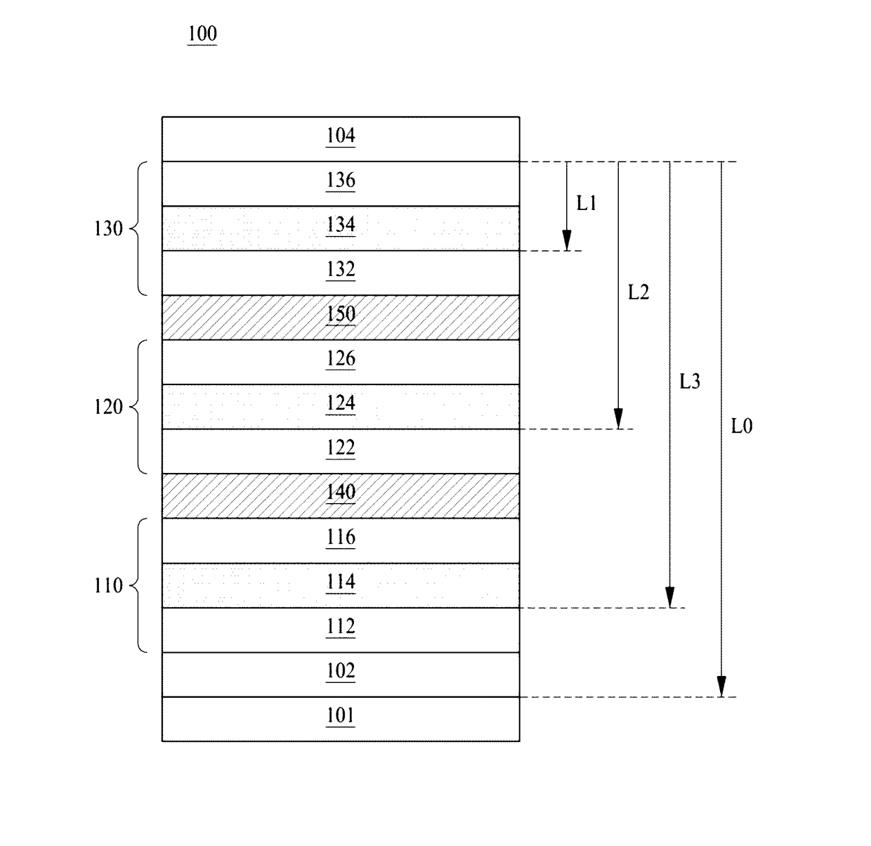
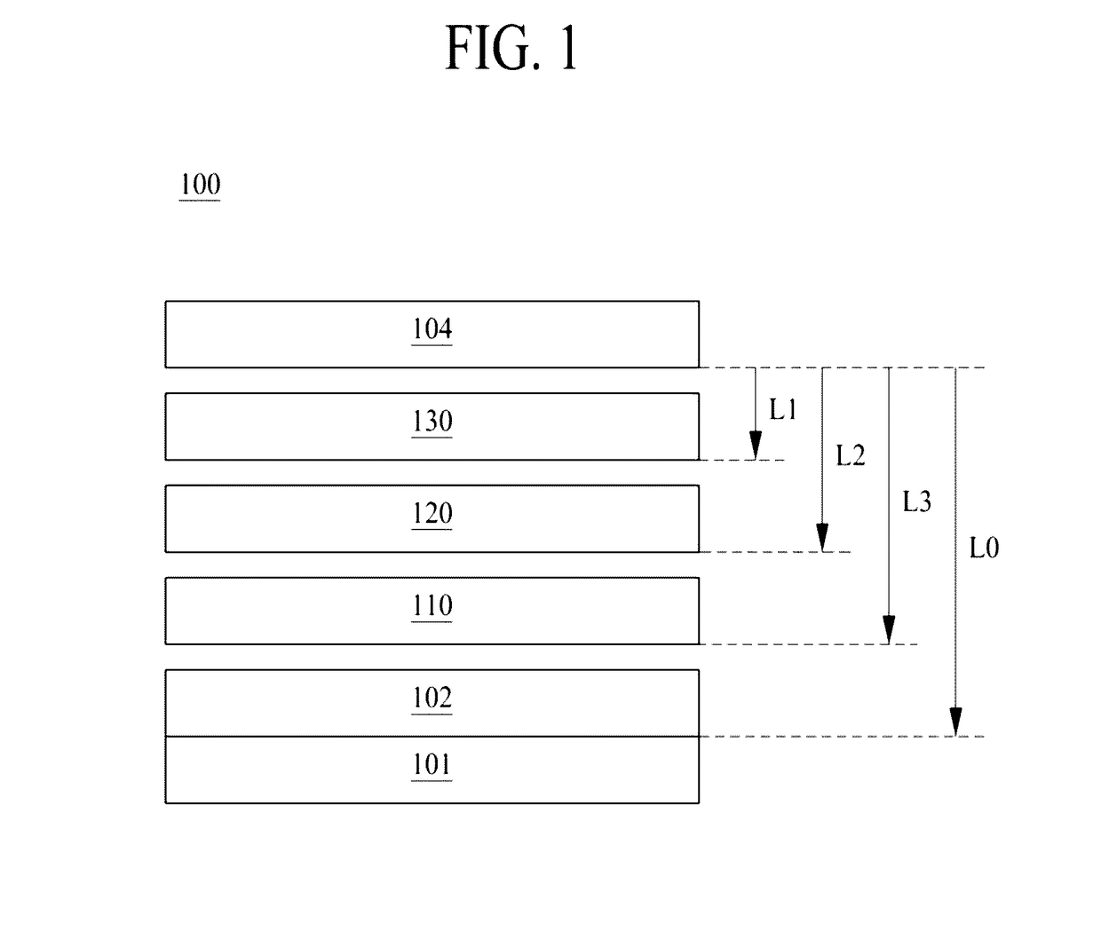
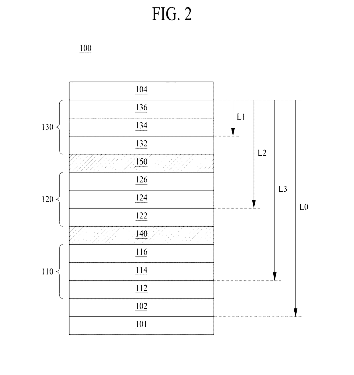
[0137]FIG. 2 is a diagram illustrating a white organic light emitting device according to the present invention.

[0138]A white organic light emitting device 100 illustrated in FIG. 2 includes first and second electrodes 102 and 104 and first to third emission parts 110, 120 and 130 between the first and second electrodes 102 and 104.

[0139]Each of the first electrode 102 and the second electrode 104 may be referred to as an anode or a cathode.

[0140]A position L0 of the first electrode 102 is set to 4,500 Å to 6,000 Å from the second electrode 104. Since the position L0 of the first electrode 102 is set, emission peaks of emission layers configuring the first to third emission parts 110, 120 and 130 are located at a specific wavelength, and light having the specific wavelength is emitted, thereby improving an emission efficiency of the emission layers. The first to third emission parts 110, 120 and 130 have the EPEL structure that has a maximum emission range in emission areas of the f...

second embodiment

[0250]FIG. 5 is a diagram illustrating a white organic light emitting device according to the present invention.

[0251]A white organic light emitting device 100 illustrated in FIG. 5 includes first and second electrodes 102 and 104 and first to third emission parts 110, 120 and 130 between the first and second electrodes 102 and 104. In describing the present embodiment, descriptions on elements which are the same as or correspond to the elements according to the preceding embodiment are not repeated. A position of the first electrode 102 is set to 4,500 Å to 6,000 Å from the second electrode 104. Also, emission peaks of emission layers configuring the first to third emission parts 110, 120 and 130 are located at a specific wavelength, and light having the specific wavelength is emitted, thereby improving an emission efficiency of the emission layers. The first to third emission parts 110, 120 and 130 have the EPEL structure that has a maximum emission range in emission areas of the ...

third embodiment

[0339]FIG. 8 is a diagram illustrating a white organic light emitting device according to the present invention.

[0340]In the present embodiment, emission positions of emission layers are set from a first electrode, and may be set from the first electrode depending on a device design.

[0341]The position of the second electrode 104 is set to within 4,500 Å to 6,000 Å from the second electrode 104. Also, emission peaks of the emission layers configuring the first to third emission parts 110, 120 and 130 are located at a specific wavelength, and light having the specific wavelength is emitted, thereby improving emission efficiency. Also, the first to third emission parts 110, 120 and 130 have the EPEL structure that has a maximum emission range in emission areas of the first to third emission layers.

[0342]The first emission part 110 may include a first HTL 112, a first EML 114, and a first ETL 116, and which are disposed on the second electrode 104.

[0343]Although not shown, an HIL may be...


PUM


Abstract

Discussed is a white organic light emitting device for enhancing emission efficiency and panel efficiency. The white organic light emitting device can include a first emission part between a first electrode and a second electrode and configured to include a first emission layer (EML), a second emission part on the first emission part and configured to include a second EML, and a third emission part on the second emission part and configured to include a third EML. The first to third emission parts have an emission position of emitting layers (EPEL) structure in which the first to third emission parts have a maximum emission range in respective emission areas of the first to third EMLs.

Description

CROSS-REFERENCE TO RELATED APPLICATIONS[0001]This application claims the priority benefit of the Korean Patent Application Nos. 10-2014-0037728 filed on Mar. 31, 2014, 10-2014-0056607 filed on May 12, 2014, 10-2014-0082617 filed on Jul. 2, 2014, and 10-2015-0030633 filed on Mar. 4, 2015, which are all hereby incorporated by reference as if fully set forth herein.BACKGROUND[0002]Field of the Invention[0003]The present invention relates to an organic light emitting device, and more particularly, to a white organic light emitting device for enhancing emission efficiency.[0004]Discussion of the Related Art[0005]Recently, as society advances to the information-oriented society, the field of display devices which visually express an electrical information signal is rapidly advancing. Flat panel display (FPD) devices, having excellent performance in terms of thinning, lightening, and low power consumption, have been developed.[0006]Examples of the FPD devices include LCD devices, plasma di...

Claims


Application Information

Patent Timeline
Patent Type & Authority Patents(United States)
IPC IPC(8): H01L51/50H01L51/52
CPCH01L51/504H01L51/5044H01L51/5265H10K50/131H10K50/13H10K50/852
Inventor SONG, KI-WOOGPIEH, SUNG HOONKAM, YOUN SEOKKIM, TAE SHICKKIM, SE UNGKIM, HYUNG JUNE
Owner LG DISPLAY CO LTD
Why Eureka
Try Eureka