Chip-on-film (COF) package, COF package array including the same, and display device including the same

a technology of chip-on-film and cof, applied in the direction of semiconductor devices, semiconductor/solid-state device details, instruments, etc., can solve the problem of shorts between adjacent interconnections, and achieve the effect of reducing or preventing the occurrence of shorts

Active Publication Date: 2017-06-27
SAMSUNG DISPLAY CO LTD
View PDF21 Cites 1 Cited by
  • Summary
  • Abstract
  • Description
  • Claims
  • Application Information

AI Technical Summary

Benefits of technology

[0008]Aspects of embodiments of the present disclosure are directed toward a chip-on-film (COF) package capable of reducing or preventing the occurrence of shorts between adjacent signal interconnections.

Problems solved by technology

Thus, a short may occur between adjacent interconnections due to a cutting process of separating COF packages, or melting or corrosion of a material of the interconnections.

Method used


Image

  • Chip-on-film (COF) package, COF package array including the same, and display device including the same
  • Chip-on-film (COF) package, COF package array including the same, and display device including the same
  • Chip-on-film (COF) package, COF package array including the same, and display device including the same

Examples


Embodiment Construction

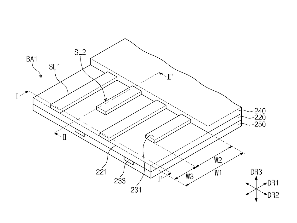
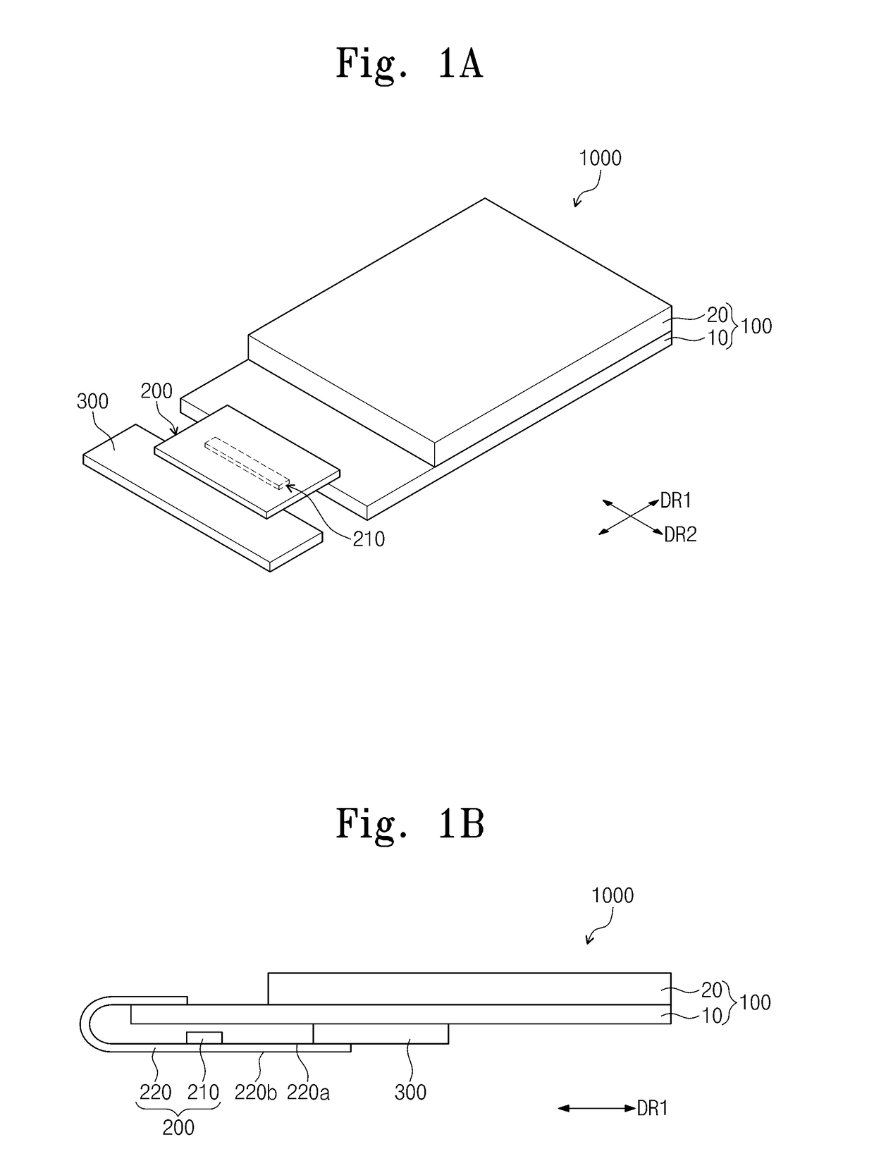
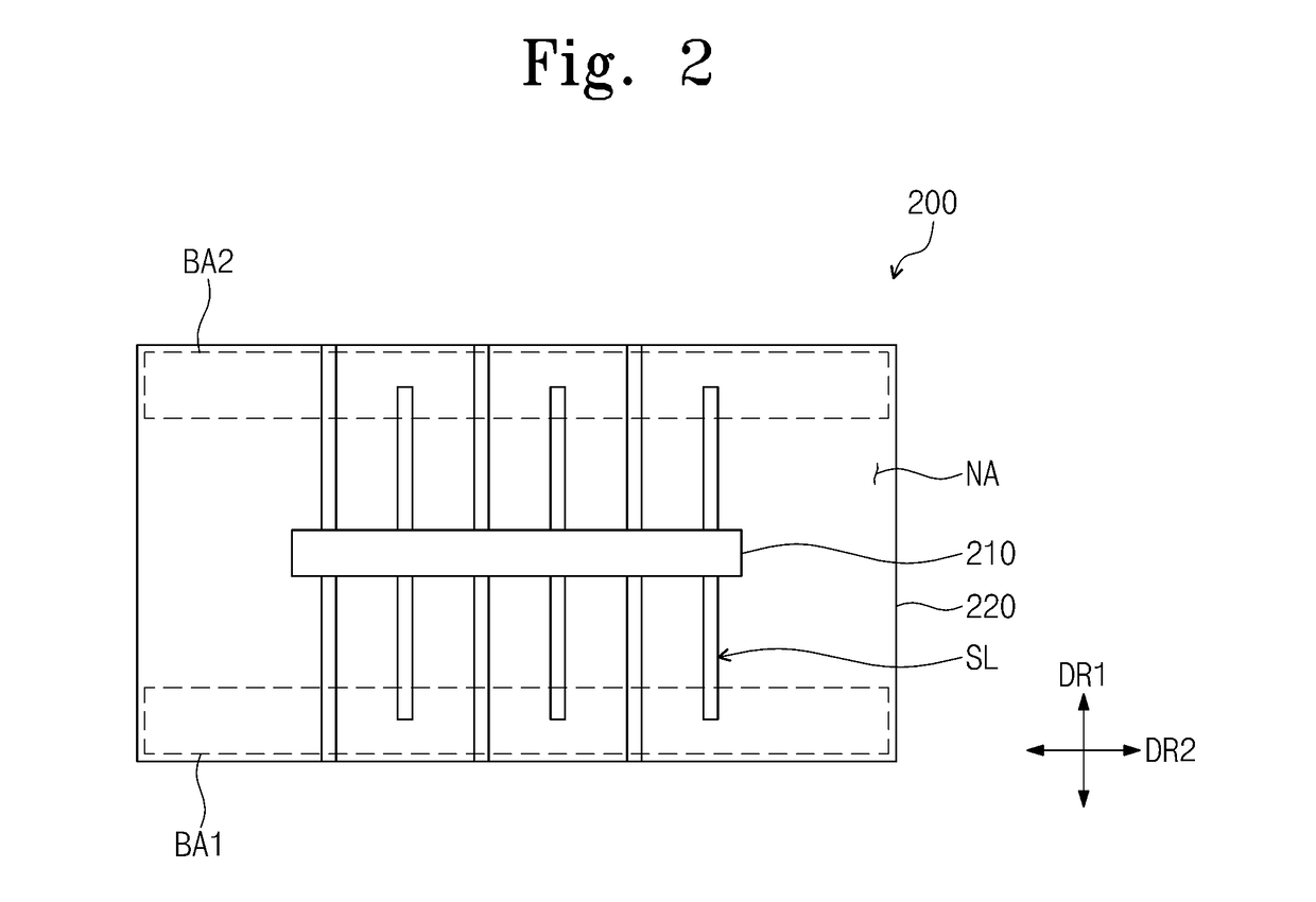
[0044]It will be understood that when an element or layer is referred to as being “on”, “connected to”, or “coupled to” another element or layer, it can be directly on, connected, or coupled to the other element or layer or intervening elements or layers may be present. In contrast, when an element is referred to as being “directly on”, “directly connected to”, or “directly coupled to” another element or layer, there are no intervening elements or layers present. Like numbers refer to like elements throughout. As used herein, the term “and / or” includes any and all combinations of one or more of the associated listed items. Further, the use of “may” when describing embodiments of the present invention refers to “one or more embodiments of the present invention.”

[0045]It will be understood that, although the terms first, second, etc. may be used herein to describe various elements, components, regions, layers, and / or sections, these elements, components, regions, layers, and / or sectio...


PUM


Abstract

A chip-on-film (COF) package includes a base film, an integrated circuit chip, and a plurality of signal interconnections. The base film includes a bonding region and a non-bonding region. The integrated circuit chip is at the non-bonding region. Each of the plurality of signal interconnections is coupled to the integrated circuit chip and extend to the bonding region along a first direction. The plurality of signal interconnections are spaced from each other along a second direction substantially crossing the first direction. The plurality of signal interconnections alternate on a first surface and a second surface opposite to the first surface of the base film along the second direction.

Description

CROSS-REFERENCE TO RELATED APPLICATION[0001]This patent application claims priority to and the benefit of Korean Patent Application No. 10-2013-0110649, filed on Sep. 13, 2013 in the Korean Intellectual Property Office, the content of which is hereby incorporated by reference in its entirety.BACKGROUND[0002]1. Field[0003]Embodiments of the present disclosure relate to a chip-on-film (COF) package, a COF package array including the same, and a display device including the same. More particularly, embodiments of the present disclosure relate to a COF package capable of reducing or preventing shorts (e.g., short circuits) between adjacent signal interconnections, a COF package array including the same, and a display device including the same.[0004]2. Description of the Related Art[0005]A display device includes a display panel, a printed circuit board driving the display panel, and a tape carrier package (TCP) or chip-on-film (COF) package electrically coupling the display panel to the...

Claims


Application Information

Patent Timeline
Patent Type & Authority Patents(United States)
IPC IPC(8): G06K9/00H01L27/15H01L23/498
CPCH01L27/156H01L23/4985H01L2924/0002H01L2924/00
Inventor KIM, DONG-HO
Owner SAMSUNG DISPLAY CO LTD
Why Eureka
Try Eureka