LED back end assembly and method of manufacturing

a technology of led back end and assembly, which is applied in the direction of light and heating apparatus, semiconductor devices for light sources, solid-state devices, etc., can solve the problems of limited alignment of led dies within apertures, reduced heat sink manufacturing costs, and reduced cost, so as to reduce costs and reduce manufacturing costs. , the effect of substantially eliminating the size of stando

Active Publication Date: 2017-08-29
FLEXTRONICS AP LLC
View PDF48 Cites 0 Cited by
  • Summary
  • Abstract
  • Description
  • Claims
  • Application Information

AI Technical Summary

Benefits of technology

[0004]Embodiments of an LED device and method of manufacture are directed to separately coupling a thin flexible interposer and an LED die to a heat sink structure and then electrically coupling the interposer and the LED die together with a wirebond. As a result, only a single interposer is necessary and problems with standoff size are substantially eliminated. Further, a specifically shaped perimeter of an aperture within the interposer negates the need for a cavity or alignment markings within the heat sink structure by limiting the orientation in which the die fits within the aperture. Thus, heat sink manufacturing cost is saved. Further, embodiments of an LED device and method of manufacture are directed to coupling a rigid circuit board to an LED die such that electrical contacts of the die are electrically coupled with electrical input / output terminals of the circuit board. This die / board unit is then able to be coupled to a heat sink structure to form a portion of the device. In particular, the rigidity of the circuit board enable an entire array of LED die / circuit boards to be simultaneously or concurrently manufactured on a single panel and then singulated. This results in assembly efficiency and therefore reduced costs. Moreover, studs or bumps are able to be fabricated on the LED dies in order to electrically couple with the terminals of the circuit board, wherein the bumps are able to provide a better standoff than previously possible.

Problems solved by technology

Further, a specifically shaped perimeter of an aperture within the interposer negates the need for a cavity or alignment markings within the heat sink structure by limiting the orientation in which the die fits within the aperture.
Thus, heat sink manufacturing cost is saved.
In some embodiments, the aperture is square or rectangular such that the alignment of the LED die within the aperture is limited.
In some embodiments, the cavity is square or rectangular such that the alignment of the die when positioned within the cavity is limited.

Method used


Image

  • LED back end assembly and method of manufacturing
  • LED back end assembly and method of manufacturing
  • LED back end assembly and method of manufacturing

Examples


Embodiment Construction

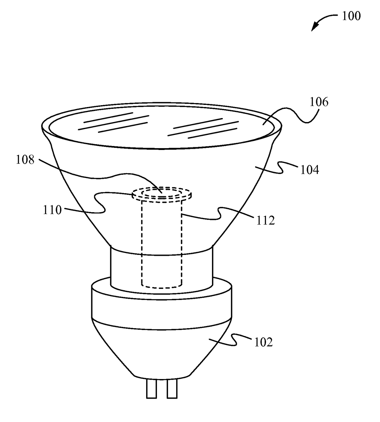
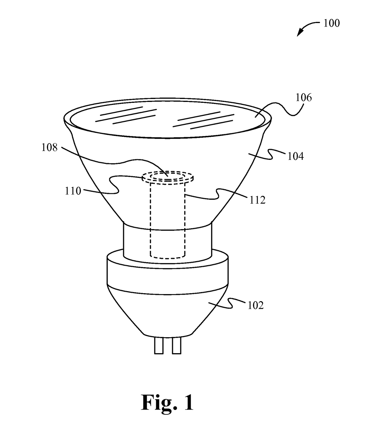
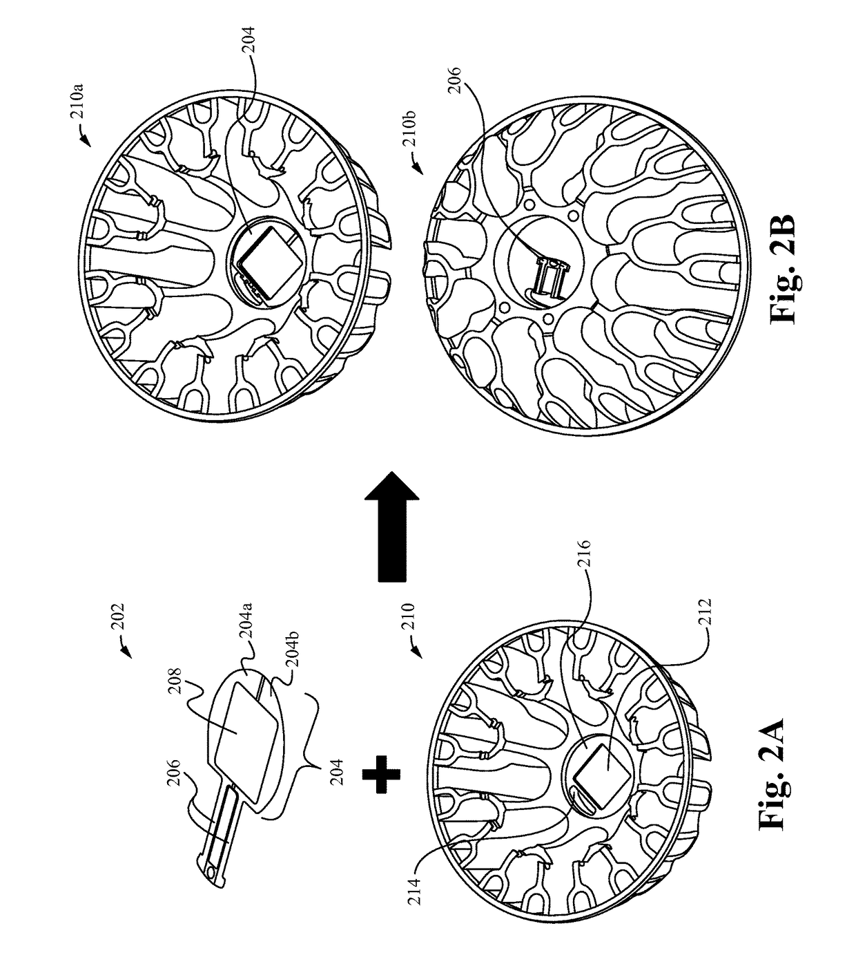
[0026]Embodiments of the present application are directed to an LED device and method of manufacture. Those of ordinary skill in the art will realize that the following detailed description of the LED device and method of manufacture is illustrative only and is not intended to be in any way limiting. Other embodiments of the power converter will readily suggest themselves to such skilled persons having the benefit of this disclosure.

[0027]Reference will now be made in detail to implementations of the LED device and method of manufacture as illustrated in the accompanying drawings. The same reference indicators will be used throughout the drawings and the following detailed description to refer to the same or like parts. In the interest of clarity, not all of the routine features of the implementations described herein are shown and described. It will, of course, be appreciated that in the development of any such actual implementation, numerous implementation-specific decisions must ...


PUM


Abstract

An LED device and method of manufacture including separately coupling a thin flexible interposer and an LED die to a heat sink structure and then electrically coupling the interposer and the LED die together with a wirebond. A specifically shaped perimeter of an aperture within the interposer negates the need for a cavity or alignment markings within the heat sink structure by limiting the orientation in which the die fits within the aperture. Alternatively, an LED device and method of manufacture include coupling a rigid circuit board to an LED die such that electrical contacts of the die are electrically coupled with electrical input / output terminals of the circuit board. This die / board unit is then able to be coupled to a heat sink structure to form a portion of the device.

Description

RELATED APPLICATIONS[0001]This Patent Application claims priority under 35 U.S.C. 119 (e) of the U.S. Provisional Application Ser. No. 61 / 770,930, filed Feb. 28, 2013, and entitled “LED Back End Assembly and Method of Manufacturing,” which is hereby incorporated by reference.FIELD OF THE INVENTION[0002]The present invention is generally directed to the field of light emitting diodes. More specifically, the present invention is directed to a light-emitting diode apparatus.BACKGROUND OF THE INVENTION[0003]A light-emitting diode (LED) is a semiconductor light source. LEDs are increasingly being used in a wide variety of lighting applications. LEDs continue growing in popularity due in part to their efficiency and extended lifetimes. An LED-based light source typically includes one or more LED dies mounted on a substrate interposer within a housing via solder. However, due to the small pad geometry of the die, the tolerances and positioning of the die / interposer within the housing can b...

Claims


Application Information

Patent Timeline
Patent Type & Authority Patents(United States)
IPC IPC(8): H01L33/00F21K9/90H01L33/64F21V29/77H01L33/62F21K9/20F21Y115/10
CPCH01L33/64F21K9/90F21K9/20F21V29/773F21Y2115/10H01L33/62H01L2924/0002H01L2924/00
Inventor TAM, SAMUELKURWA, MURADPANG TAK, SHING DICK
Owner FLEXTRONICS AP LLC
Why Eureka
Try Eureka