Package substrate machining method

a technology of machining method and package substrate, which is applied in the direction of electrical apparatus, semiconductor/solid-state device manufacturing, and semiconductor devices. it can solve the problems of stuck molten material in the groove, and achieve the effect of simple cleaning step

Active Publication Date: 2017-11-28
DISCO CORP
View PDF4 Cites 2 Cited by
  • Summary
  • Abstract
  • Description
  • Claims
  • Application Information

AI Technical Summary

Benefits of technology

[0007]In light of the foregoing, it is an object of the present invention to provide a package substrate machining method that prevents sticking of a molten material to device packages.
[0010]In the package substrate machining method according to the present invention, the second laser-machined grooves are formed by irradiating a laser beam from the ceramic substrate side of the package substrate after formation of the first laser-machined grooves in the resin coating layer that covers the ceramic substrate. Therefore, the majority of the molten material produced from the ceramic substrate is accommodated in the first laser-machined grooves formed in the coating layer. The coating layer is made of a resin. This makes it unlikely that the molten material produced from the ceramic substrate may become stuck in the first laser-machined grooves. As a result, the molten material can be removed by a simple cleaning step. Thus, the package substrate machining method according to the present invention prevents sticking of a molten material formed as a result of machining of a package substrate to device packages.

Problems solved by technology

However, although the above method makes it less likely for the molten material to stick to the rear face side of the ceramic substrate, the molten material accommodated in the grooves remains and becomes stuck in an as-is manner on side faces of the device packages obtained by dividing the package substrate.

Method used


Image

  • Package substrate machining method
  • Package substrate machining method
  • Package substrate machining method

Examples


Embodiment Construction

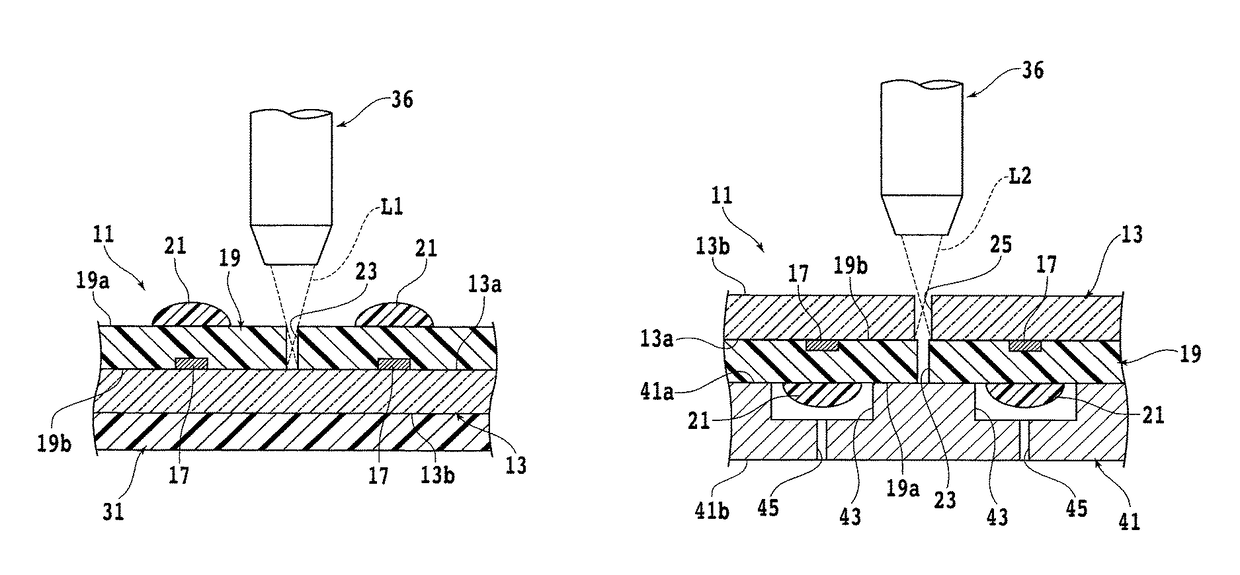
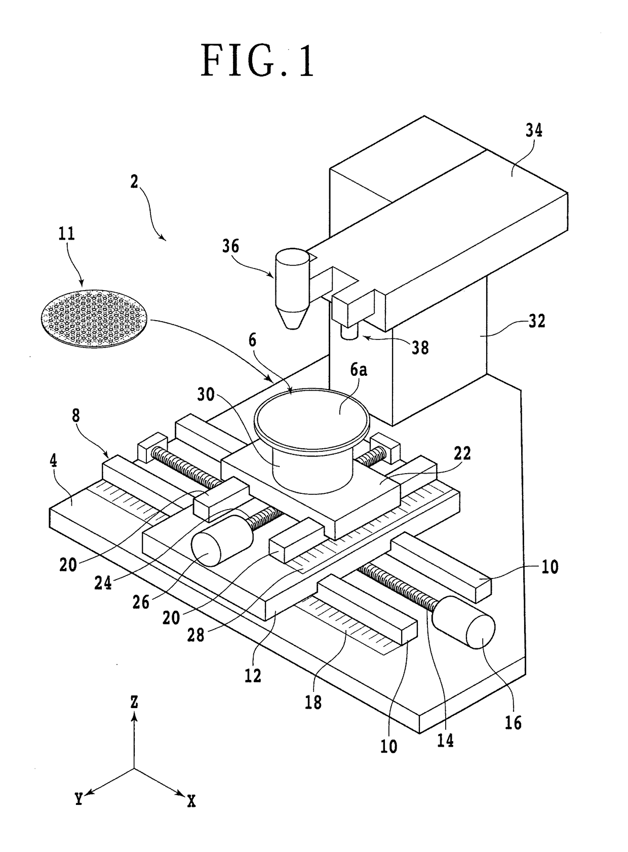
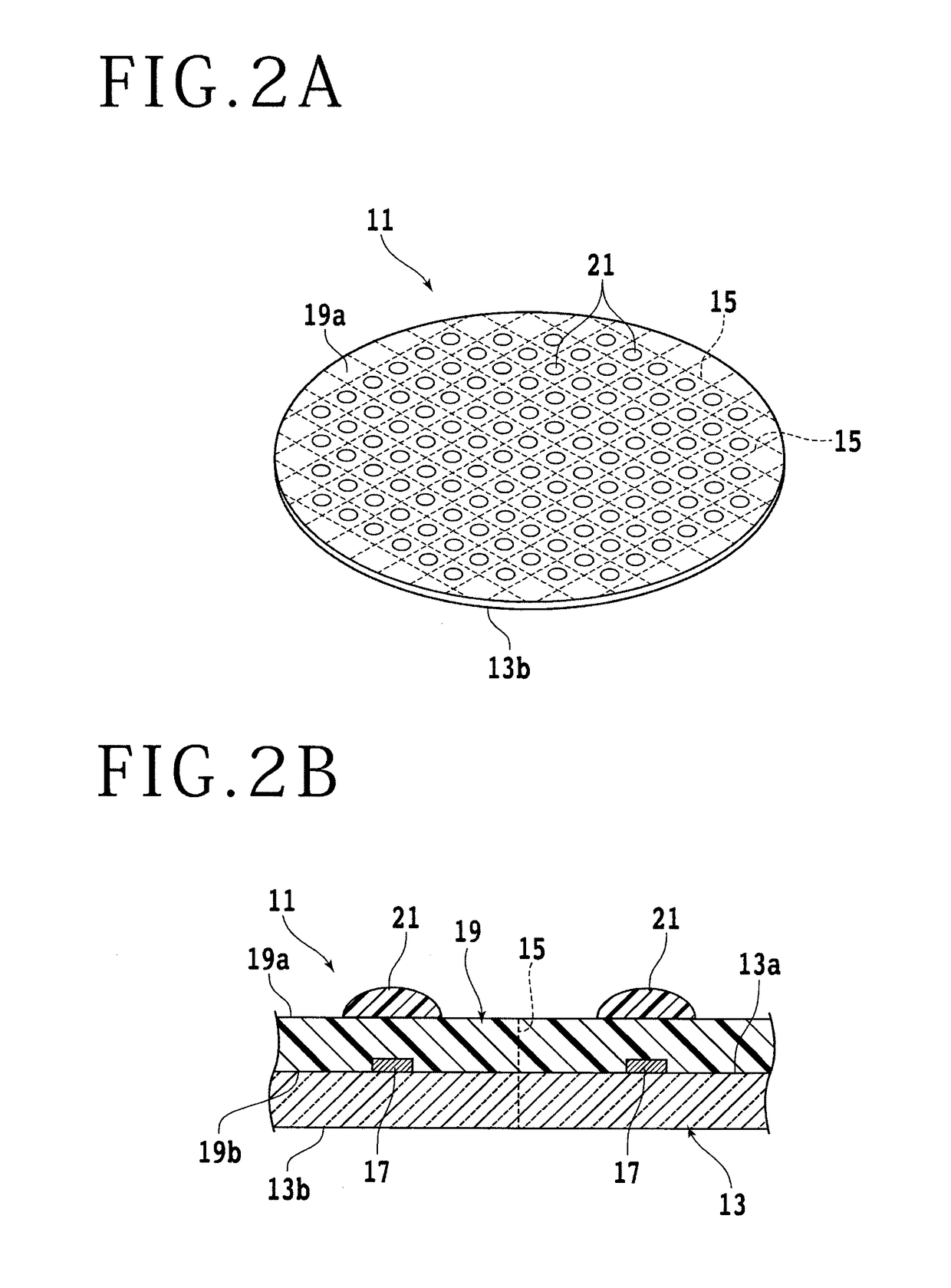
[0017]A description will be given of an embodiment of the present invention with reference to the accompanying drawings. A package substrate machining method according to the present embodiment includes a first laser-machined groove formation step (refer to FIG. 3A), a second laser-machined groove formation step (refer to FIG. 3B), and a cleaning step. In the first laser-machined groove formation step, first laser-machined grooves are formed in a resin coating layer along scheduled division lines (streets) set up in a package substrate by irradiating a laser beam at a wavelength readily absorbed by the coating layer. The coating layer covers a first face of a ceramic substrate. It should be noted that the first laser-machined grooves are formed in such a manner as to reach an interface with the ceramic substrate from a front face side where the coating layer is exposed. In the second laser-machined groove formation step, second laser-machined grooves are formed along the scheduled d...


PUM

PropertyMeasurementUnit
thicknessaaaaaaaaaa
thicknessaaaaaaaaaa
wavelengthaaaaaaaaaa

Abstract

A package substrate machining method is provided. The package substrate includes a ceramic substrate, a plurality of device chips arranged on one face of the ceramic substrate, and a coating layer made of a resin that covers the entire one face of the ceramic substrate. The package substrate machining method includes a first laser-machined groove formation step adapted to form, in the coating layer, first laser-machined grooves along scheduled division lines set up on the package substrate by irradiating a laser beam at a wavelength absorbable by the coating layer from the coating layer side of the package substrate; and a second laser-machined groove formation step adapted to form, in the ceramic substrate and after the first laser-machined groove formation step, second laser-machined grooves along the scheduled division lines by irradiating a laser beam from the ceramic substrate side of the package substrate.

Description

BACKGROUND OF THE INVENTION[0001]Field of the Invention[0002]The present invention relates to a machining method of a package substrate having light emitting diodes (LEDs) or other chips sealed thereon.[0003]Description of the Related Art[0004]When LEDs or other chips are packaged, a plurality of device chips are arranged on a front face of a ceramic substrate made, for example, of Al2O3 first, and a front face side of this ceramic substrate is coated with a light-transmitting mold resin, thus forming a package substrate. A plurality of device packages, each having a device chip packaged, can be obtained by dividing the package substrate along scheduled division lines (streets) set up between adjacent device chips.[0005]The above division of a package substrate is conducted, for example, by a method based on abrasion using laser beams. However, this method highly likely results in degraded device chip quality due to sticking of a molten material, produced by abrasion, to a rear face...

Claims


Application Information

Patent Timeline
Patent Type & Authority Patents(United States)
IPC IPC(8): H01L33/00
CPCH01L33/0095H01L21/268H01L21/3043H01L33/005H01L2933/005H01L33/02H01L33/48H01L21/76H01L2933/0041H01L2924/12041
Inventor YOSHIDA, YUTA
Owner DISCO CORP
Why Eureka
Try Eureka