
Touch display substrate, electronic device and driving method

a technology of electronic devices and substrates, applied in the field of touch displays, can solve the problems of low production efficiency, high cost, and large thickness, and achieve the effects of improving touch detection accuracy, reducing vertical crosstalk, and reducing production costs

Active Publication Date: 2017-12-12
SHANGHAI TIANMA MICRO ELECTRONICS CO LTD +1
View PDF30 Cites 8 Cited by
  • Summary
  • Abstract
  • Description
  • Claims
  • Application Information

AI Technical Summary

Benefits of technology

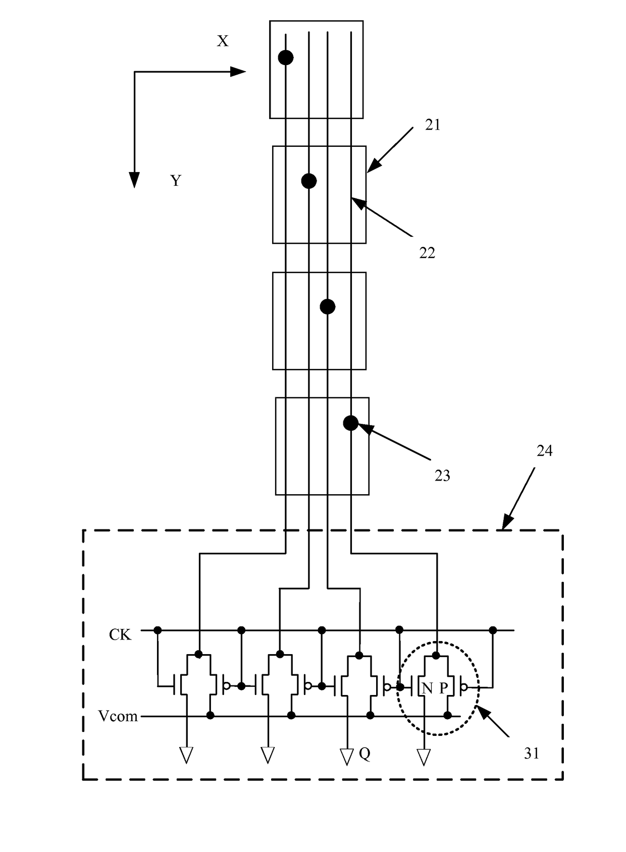
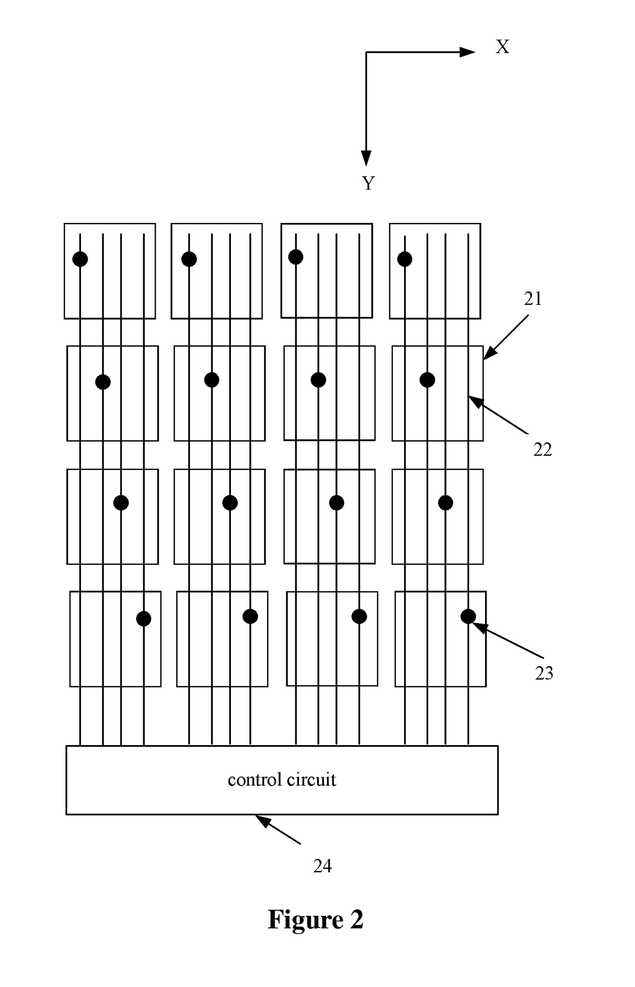
The present invention provides a touch display substrate, an electronic device and a driving method that can reduce vertical crosstalk and improve the accuracy of touch detection. This is achieved by designing a phase difference between touch detection signals for at least two wires to cancel out interferences and improve touch detection accuracy. The electronic device using this touch display substrate also has good accuracy of touch detection. This technology can make the touch screen more accurate and reliable.

Problems solved by technology

Using known technologies, the touch panel and the display panel are fabricated independently, resulting in high cost, great thickness, and low production efficiency.
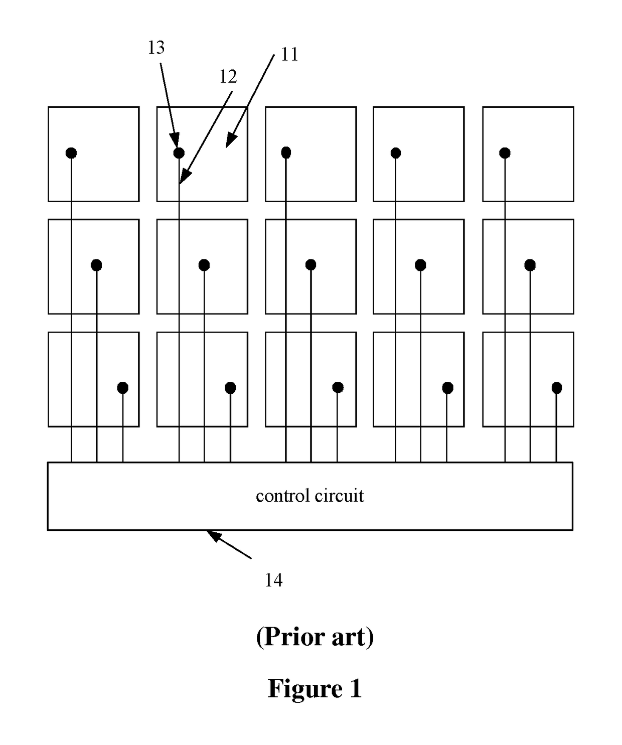
A touch detection signal transmitted in wire 12 may be coupled to other common electrodes in the same column via parasitic capacitances, thereby resulting in serious vertical crosstalk and affecting the accuracy of the touch detection.

Method used


Image

  • Touch display substrate, electronic device and driving method
  • Touch display substrate, electronic device and driving method
  • Touch display substrate, electronic device and driving method

Examples


Embodiment Construction

[0025]The technical solutions according to the embodiments of the present disclosure are described clearly and completely as follows in conjunction with the drawings. It is apparent that the described embodiments are only a few rather than all of the embodiments according to the present disclosure. Any other embodiments obtained by those skilled in the art based on the embodiments in the present disclosure without any creative work fall in the scope of the present disclosure.

[0026]As described in the background, in FIG. 1, wire 12 is connected to a common electrode 11 at a distal end (an end of the column far away from the control circuit 14) and wire 12 is also connected to a touch detection amplifier 14 by striding over other common electrodes in the same column. In this case, a touch detection signal transmitted in wire 12 may be inadvertently coupled to other common electrodes in the same column via parasitic capacitances, resulting in serious vertical crosstalk and affecting th...


PUM


Abstract

Provided are a touch display substrate, an electronic device and a driving method. The touch display substrate includes a common electrode layer and a wire layer arranged opposite to each other. The common electrode layer includes multiple common electrodes arranged in an array. The wire layer includes multiple wires connected to the common electrodes in a one-to-one way. The wires do not intersect with one another and are for inputting touch detection signals to the common electrodes, the wires extend in the same direction and touch detection signals are input to the wires simultaneously, and a phase difference between touch detection signals for at least two adjacent wires is 180 degrees. Interferences on one common electrode from the two wires, for which the touch detection signals have a phase difference of 180 degrees, may cancel each other out, thereby attenuating vertical crosstalk and improving the accuracy of touch detection.

Description

CROSS REFERENCE OF RELATED APPLICATION[0001]The present application claims the priority to Chinese Patent Application No. 201510486242.0, titled “TOUCH DISPLAY SUBSTRATE, ELECTRONIC DEVICE AND DRIVING METHOD”, filed on Aug. 10, 2015 with the State Intellectual Property Office of the People's Republic of China, the content of which is incorporated herein by reference in its entirety.FIELD[0002]The present disclosure relates to the technical field of touch display, and in particular, to a touch display substrate, an electronic device and a driving method.BACKGROUND[0003]At the initial stage of development of touch display technology, a touch display panel is formed by a combination of a touch panel and a display panel to achieve touch display function. Using known technologies, the touch panel and the display panel are fabricated independently, resulting in high cost, great thickness, and low production efficiency.[0004]With the development of the self-contained touch display technolo...

Claims


Application Information

Patent Timeline
Patent Type & Authority Patents(United States)
IPC IPC(8): G06F3/041G06F3/044
CPCG06F3/0412G06F3/0416G06F3/044G09G2300/0426G02F1/13338G02F1/134336G02F1/136286G06F3/04166G06F3/0443G06F3/04164
Inventor HUANG, ZHONGSHOUCAO, ZHAOKENG
Owner SHANGHAI TIANMA MICRO ELECTRONICS CO LTD
Learn More