Unlock instant, AI-driven research and patent intelligence for your innovation.

Wear leveling of a memory array

a technology of memory array and wear leveling, applied in the direction of memory adressing/allocation/relocation, instruments, input/output to record carriers, etc., can solve the problems of limiting the useful life (or “endurance”) of blocks of nand flash memory, memory cells, and high voltage applied during program and erase operations

Active Publication Date: 2018-01-02
INT BUSINESS MASCH CORP
View PDF22 Cites 7 Cited by
  • Summary
  • Abstract
  • Description
  • Claims
  • Application Information

AI Technical Summary

Problems solved by technology

Over time, the high voltages applied during the program and erase operations tend to degrade the gate oxide of the floating gates of the transistors forming the memory cells of the blocks.
This damage to the memory cells, often referred to as “wear,” limits the useful lifetime (or “endurance”) of blocks of NAND flash memory, where endurance is typically expressed as the number of program / erase (P / E) cycles for which a block can be utilized prior to the number of errors occurring in the block reaching the level that the block is no longer useful for storing data.

Method used


Image

  • Wear leveling of a memory array
  • Wear leveling of a memory array
  • Wear leveling of a memory array

Examples


Embodiment Construction

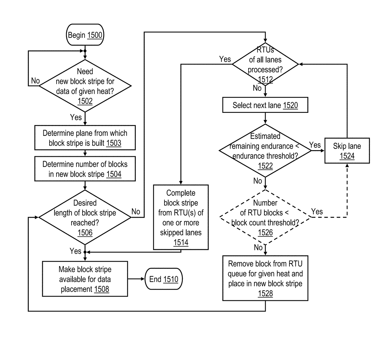
[0025]With reference to the figures and with particular reference to FIG. 1A, there is illustrated a high level block diagram of an exemplary data processing environment 100 including a data storage system 120 having a non-volatile memory array as described further herein. As shown, data processing environment 100 includes one or more hosts, such as a processor system 102 having one or more processors 104 that process instructions and data. Processor system 102 may additionally include local storage 106 (e.g., dynamic random access memory (DRAM) or disks) that may store program code, operands and / or execution results of the processing performed by processor(s) 104. In various embodiments, processor system 102 can be, for example, a mobile computing device (such as a smartphone or tablet), a laptop or desktop personal computer system, a server computer system (such as one of the POWER series available from International Business Machines Corporation), or a mainframe computer system. ...


PUM


Abstract

In at least one embodiment, a controller of a non-volatile memory array including a plurality of subdivisions stores write data within the non-volatile memory array utilizing a plurality of block stripes of differing numbers of blocks, where all of the blocks within each block stripe are drawn from different ones of the plurality of subdivisions. The controller builds new block stripes for storing write data from blocks selected based on estimated remaining endurances of blocks in each of the plurality of subdivisions.

Description

BACKGROUND OF THE INVENTION[0001]This disclosure relates to data processing and storage, and more specifically, to management of a data storage system, such as a flash memory system, to promote storage system endurance through wear leveling.[0002]NAND flash memory is an electrically programmable and erasable non-volatile memory technology that stores one or more bits of data per memory cell as a charge on the floating gate of a transistor. In a typical implementation, a NAND flash memory array is organized in blocks (also referred to as “erase blocks”) of physical memory, each of which includes multiple physical pages each in turn containing a multiplicity of memory cells. By virtue of the arrangement of the word and bit lines utilized to access memory cells, flash memory arrays can generally be programmed on a page basis, but are erased on a block basis.[0003]As is known in the art, blocks of NAND flash memory must be erased prior to being programmed with new data. A block of NAND ...

Claims


Application Information

Patent Timeline
Patent Type & Authority Patents(United States)
IPC IPC(8): G06F3/06G06F12/02
CPCG06F3/061G06F3/0655G06F12/0246G06F3/0688G06F2212/7211G06F3/0665G06F3/065G06F3/0619
Inventor FISHER, TIMOTHY J.FRY, AARON D.IOANNOU, NIKOLASKOLTSIDAS, IOANNISMA, JASONPLETKA, ROMAN A.SIMMONS, LINCOLN T.TOMIC, SASA
Owner INT BUSINESS MASCH CORP