Ring bus structure and its use in flash memory systems

a ring bus and flash memory technology, applied in the field of bus structures, can solve the problems of limiting system operating frequency, adversely affecting system performance, and restricted operating speed of flash memory systems, and achieve the effect of flexible and parallel node-to-node commands, data transfers, and easy checking

Active Publication Date: 2006-02-09
SANDISK TECH LLC
View PDF47 Cites 395 Cited by
  • Summary
  • Abstract
  • Description
  • Claims
  • Application Information

AI Technical Summary

Benefits of technology

[0017] As a further feature, the integrity of the data read from the memory may easily be checked by passing it through an error correction function typically provided by the controller, most conveniently by a circuit dedicated to executing an error correction code (ECC). If the data are transferred completely around the ring, as is preferred, they will always pass through the controller node, no matter where the source and destination nodes are located relative to that of the controller. The node originating the data transfer may optionally also verify the data received after traveling around the bus with the data it placed on the bus, in order to assure that the data were not corrupted by the transmission.
[0018] As a yet another feature, various functions and components of the controller may also be individually connected through nodes to the system ring bus, including the processor, buffer memory and ECC circuitry. The flexibility and parallelism of node-to-node command and data transfers are then further increased. A conventional controller bus may also be included for the transfer of commands and data directly among the controller components for its efficient operation when other components of the memory system are not involved.

Problems solved by technology

The controller typically suspends its primary function of transferring data into and out of the memory when performing garbage collection, thus potentially adversely affecting system performance.
The operating speed of flash memory systems is being restricted by the use of such a bus.
Since the single bus is rather long, the system operating frequency is limited by round trip delays and a large capacitive load inherent in the bus.

Method used


Image

  • Ring bus structure and its use in flash memory systems
  • Ring bus structure and its use in flash memory systems
  • Ring bus structure and its use in flash memory systems

Examples


Embodiment Construction

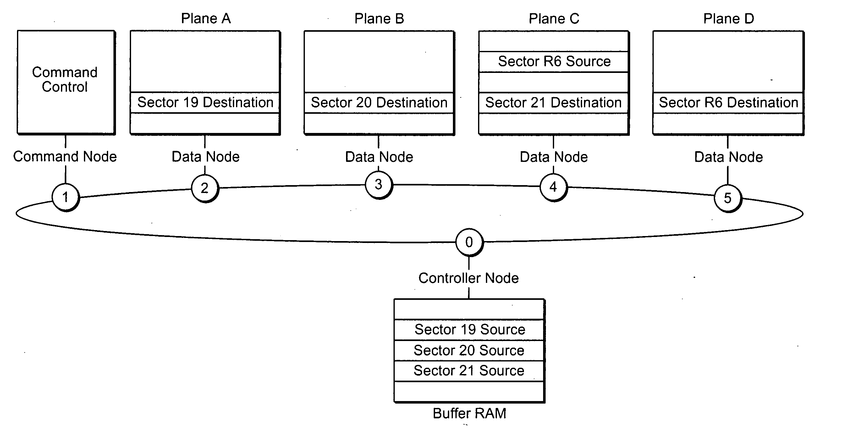
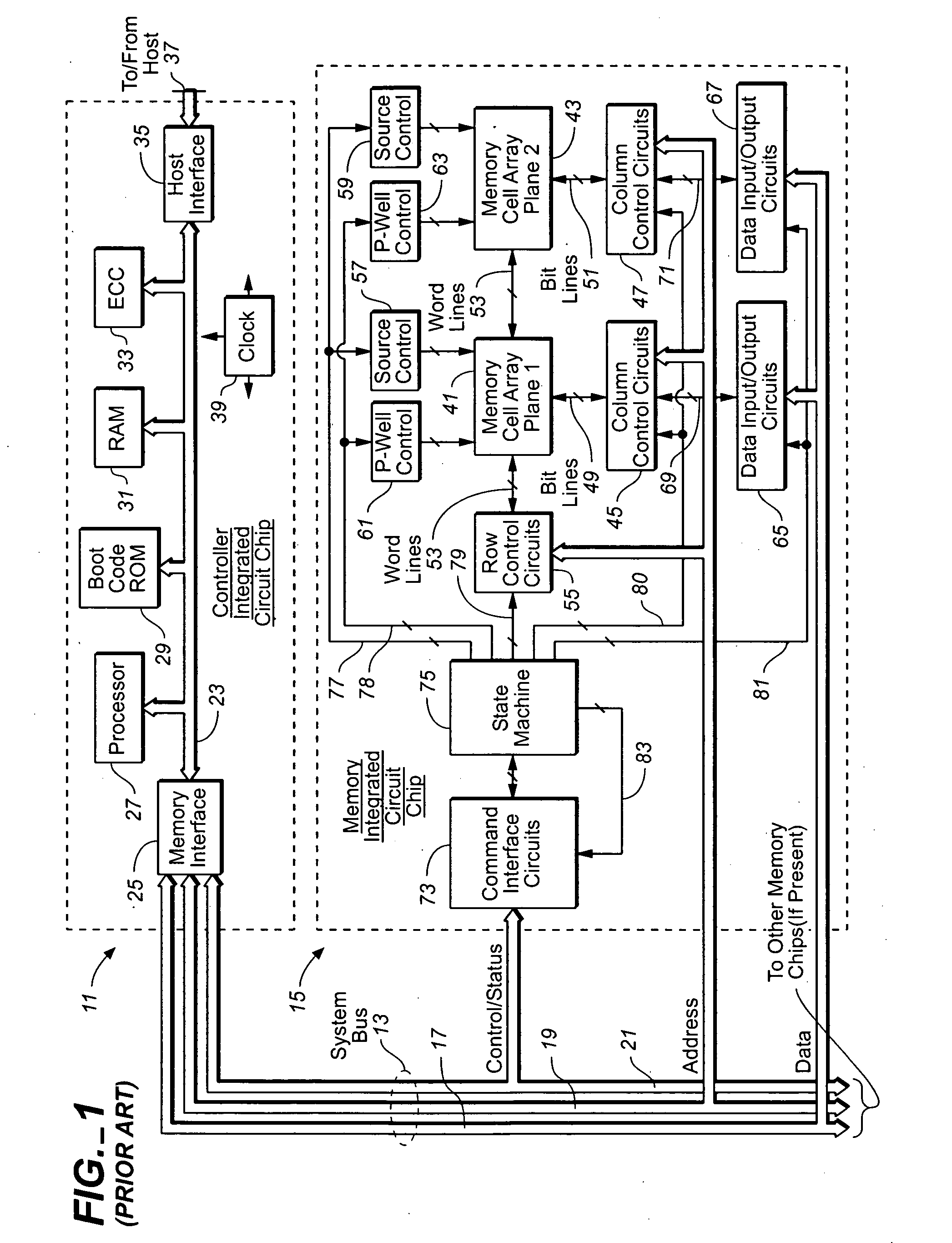
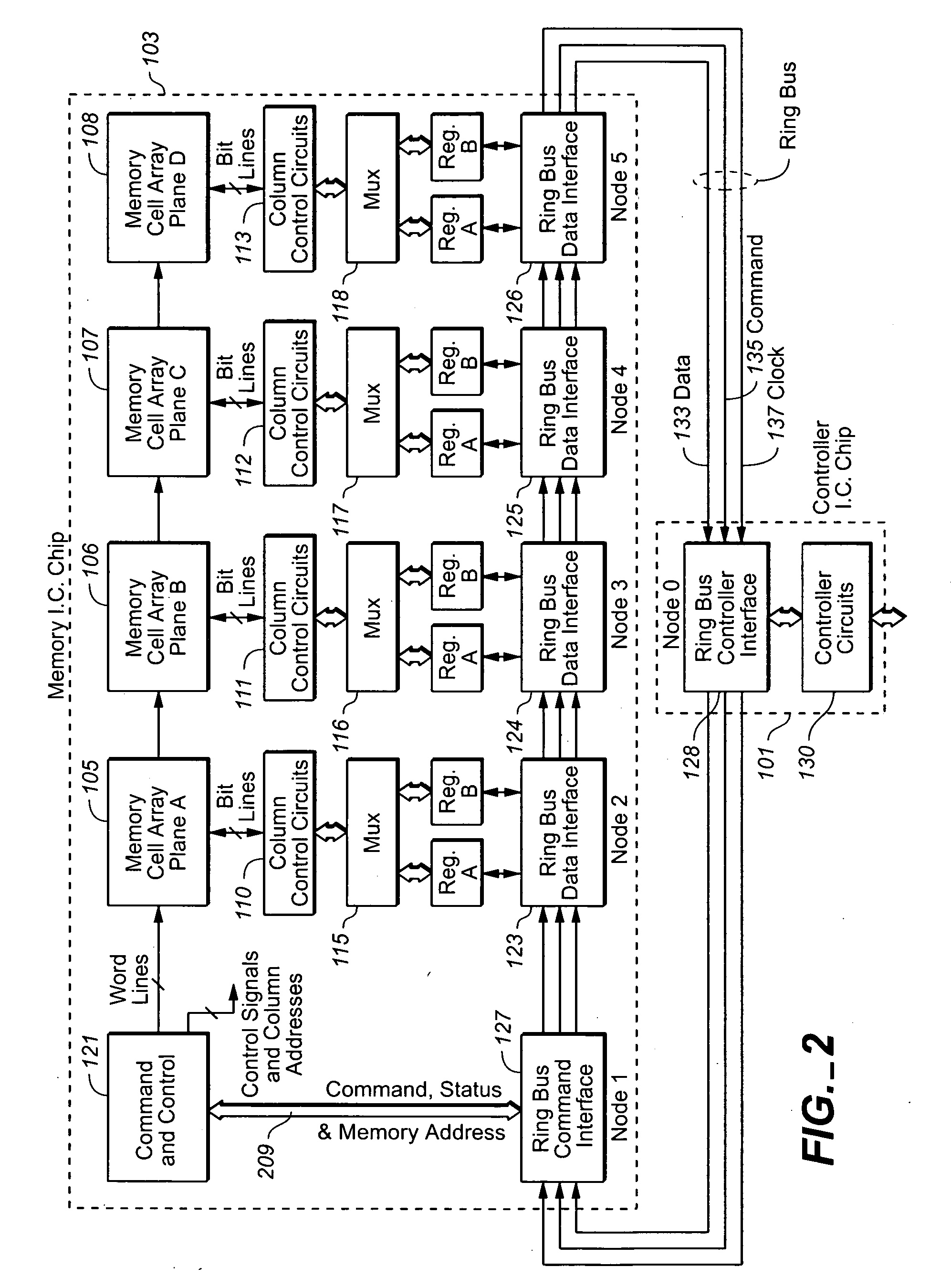
[0044] A first embodiment of a memory system using a ring bus instead of the conventional bus 15 described above is illustrated in FIGS. 2-9. Referring initially to FIG. 2, a controller integrated circuit chip 101 and a single memory chip 103 form the memory system but additional memory chips can also be included. The memory chip 103 is illustrated to have four planes 105-108 of memory cells but fewer, even one, or more than four memory planes may be used instead. Column control circuits 110-113 are connected to the respective planes 105-108. Data are programmed into and read from the memory planes 105-108 through respective multiplexing circuits 115-118 that selects one of two data registers A or B. During data programming, data stored in one of the registers A or B of a particular plane that is selected by its multiplexer is programmed into that plane. Similarly, during data reading, data read from a plane is written into one of the registers A or B selected by its multiplexer. Us...


PUM


Abstract

A system and integrated circuit chips used in the system utilize a bus in the form of a ring to interconnect nodes of individual components for transfer of data and commands therebetween. An example system described is a memory having one or more re-programmable non-volatile memory cell arrays connected to each other and to a system controller by a ring bus.

Description

BACKGROUND [0001] The present invention relates generally to bus structures and their operation in electronic systems to communicate between components of such systems, and, more specifically, to the use of a ring bus to do so, particularly in flash memory systems. [0002] There are many commercially successful re-programmable non-volatile memory products being used today, particularly in the form of small form factor cards, which employ an array of flash EEPROM (Electrically Erasable and Programmable Read Only Memory) cells formed on one or more integrated circuit chips. A memory controller, usually but not necessarily on a separate integrated circuit chip, interfaces with a host to which the card is removably connected and controls operation of the memory array within the card. Such a controller typically includes a microprocessor, some non-volatile read-only-memory (ROM), a volatile random-access-memory (RAM) and one or more special circuits such as one that calculates an error-co...

Claims


Application Information

Patent Timeline
Patent Type & Authority Applications(United States)
IPC IPC(8): G06F15/16
CPCG06F13/42G06F13/40G06F15/16
Inventor SINCLAIR, ALAN WELSH
Owner SANDISK TECH LLC
Why Eureka
Try Eureka