

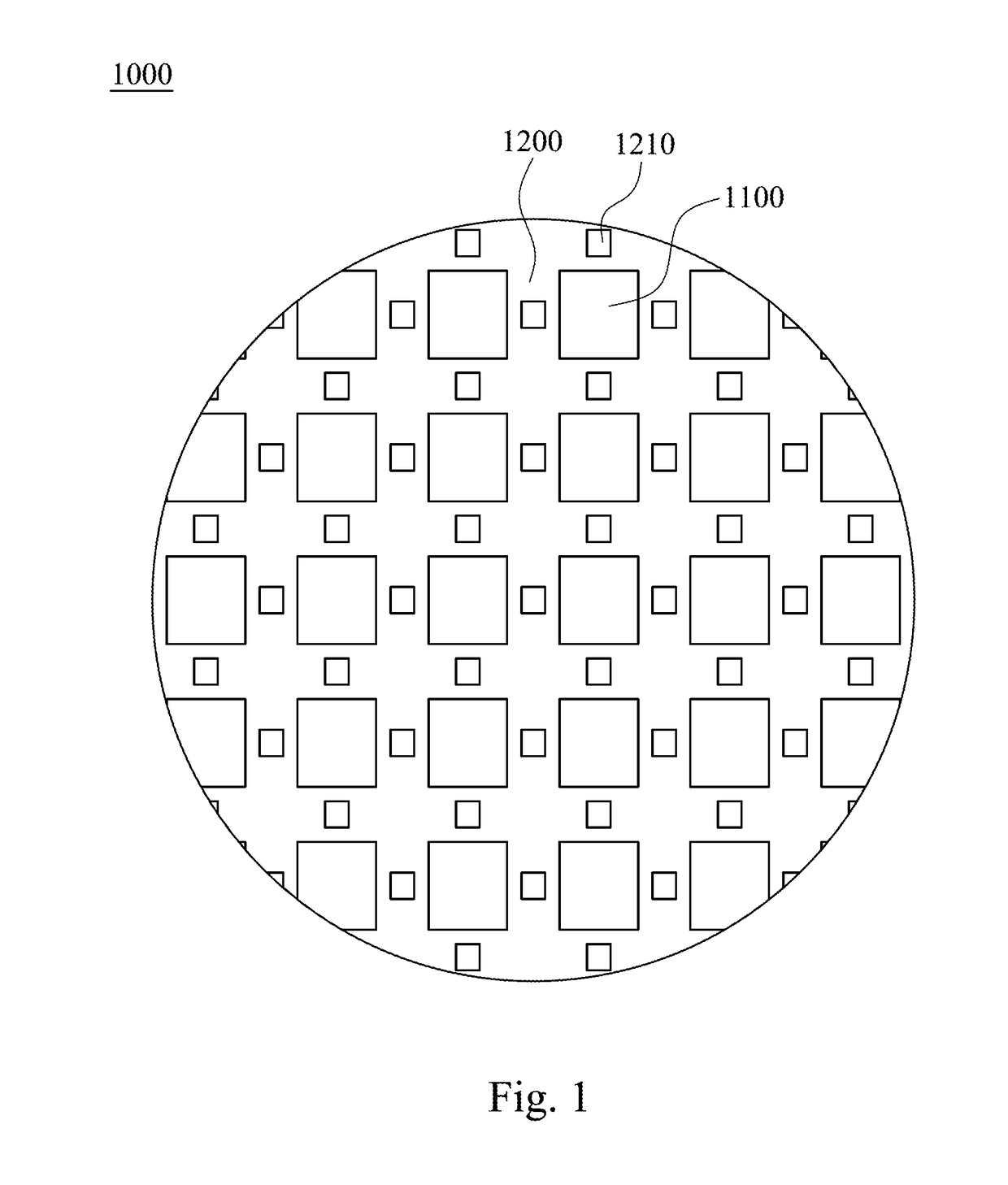
Wafers having a die region and a scribe-line region adjacent to the die region
a technology of die region and die region, applied in the field of wafers, can solve the problems of significant reliability risks, cracks extending laterally, and generation of cracks, and achieve the most significant limitation of minimizing circuit chips and reducing the number of cracks
- Summary
- Abstract
- Description
- Claims
- Application Information
AI Technical Summary
Benefits of technology
Problems solved by technology
Method used
Image

Examples
Embodiment Construction
[0033]Reference will now be made in detail to the present embodiments of the invention, examples of which are illustrated in the accompanying drawings. Wherever possible, the same reference numbers are used in the drawings and the description to refer to the same or like parts.
[0034]The following embodiments are disclosed with accompanying diagrams for detailed description. For illustration clarity, many details of practice are explained in the following descriptions. However, it should be understood that these details of practice do not intend to limit the present invention. That is, these details of practice are not necessary in parts of embodiments of the present invention. Furthermore, for simplifying the drawings, some of the conventional structures and elements are shown with schematic illustrations.
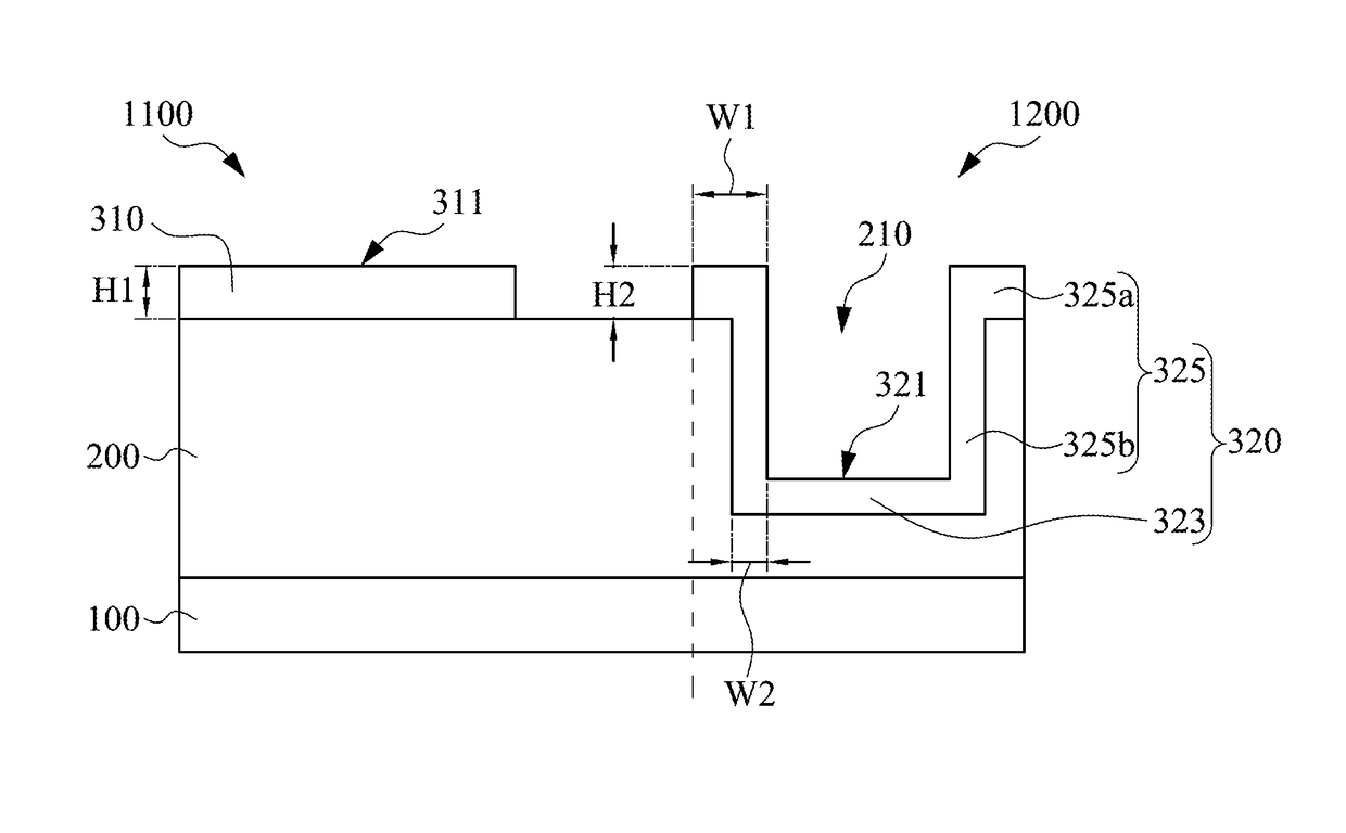
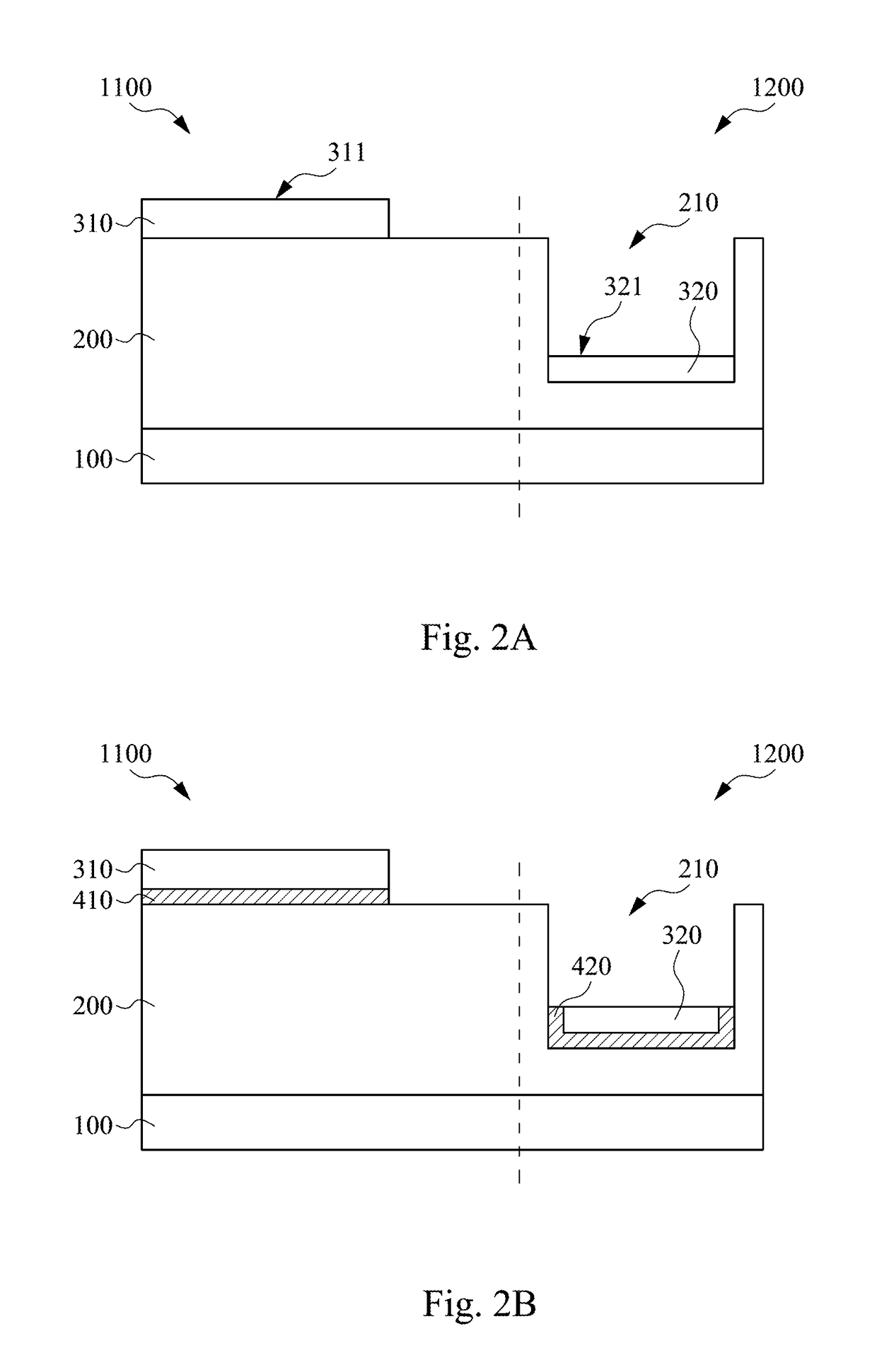
[0035]As aforementioned problems, the generation of cracks during the dicing process is a crucial problem to affect the yield of the integrated circuit (IC). Accordingly, an improv...
PUM
 Abstract
Description
Claims
Application Information