Method of producing silicon carbide epitaxial substrate, silicon carbide epitaxial substrate, and silicon carbide semiconductor device

a technology of epitaxial substrate and silicon carbide, which is applied in the direction of semiconductor devices, electrical equipment, basic electric elements, etc., can solve the problems of affecting no practical use producing means have not been established, and hole-like surface defects, so as to reduce the reliability of oxide films, the yield of sic epitaxial substrates is affected, and the growth time is longer

Inactive Publication Date: 2017-06-22
SUMITOMO ELECTRIC IND LTD
View PDF3 Cites 0 Cited by
  • Summary
  • Abstract
  • Description
  • Claims
  • Application Information

AI Technical Summary

Benefits of technology

[0007](i) A thicker epitaxial layer means a longer growth time. An epitaxial layer is grown on a substrate placed in, for example, a CVD (Chemical Vapor Deposition) furnace. However, when growth time becomes long, the crystal source material is also deposited on the inner wall of the CVD furnace, and the deposit falls on the epitaxial layer that is growing, with the result that the foreign matter is embedded in the epitaxial layer or a portion thereof falls off together with the grown crystal to cause a hole-like surface defect (also referred to as “downfall”). The downfall is a critical defect for semiconductor devices, and greatly affects yield of SiC epitaxial substrates.
[0008](ii) For SiC, there are various type of polytypes but 4H type SiC crystal (4H-SiC) is considered to be the most useful for semiconductor devices. In general, for growth of a SiC epitaxial layer, step-flow growth, which is lateral growth from an atomic level step on a substrate with a slight off angle, is performed to suppress inclusion of a different type of polytype (polytype other than the intended polytype). However, when growing a thick epitaxial layer by the step-flow growth, a fast-growing step reaches a slow-growing step and is combined therewith to form a large bunch, i.e., step-bunching takes place inevitably. The step-bunching is a factor that decreases reliability of an oxide film in a semiconductor device.
[0013]In view of the above-described problems, it is an object to provide a silicon carbide epitaxial substrate having a high-quality and thick epitaxial layer.

Problems solved by technology

However, for growing a thick SiC epitaxial layer, no producing means for practical use has not been established yet due to the following problems (i) to (iii).
However, when growth time becomes long, the crystal source material is also deposited on the inner wall of the CVD furnace, and the deposit falls on the epitaxial layer that is growing, with the result that the foreign matter is embedded in the epitaxial layer or a portion thereof falls off together with the grown crystal to cause a hole-like surface defect (also referred to as “downfall”).
The downfall is a critical defect for semiconductor devices, and greatly affects yield of SiC epitaxial substrates.
However, when growing a thick epitaxial layer by the step-flow growth, a fast-growing step reaches a slow-growing step and is combined therewith to form a large bunch, i.e., step-bunching takes place inevitably.
The step-bunching is a factor that decreases reliability of an oxide film in a semiconductor device.

Method used


Image

  • Method of producing silicon carbide epitaxial substrate, silicon carbide epitaxial substrate, and silicon carbide semiconductor device
  • Method of producing silicon carbide epitaxial substrate, silicon carbide epitaxial substrate, and silicon carbide semiconductor device
  • Method of producing silicon carbide epitaxial substrate, silicon carbide epitaxial substrate, and silicon carbide semiconductor device

Examples


first embodiment

Method for Producing Silicon Carbide Epitaxial Substrate

[0073]A first embodiment presents a method of producing a SiC epitaxial substrate including a SiC single crystal substrate and a SiC layer epitaxially grown thereon. This production method includes a first production method, a second production method, and a third production method as follows.

[0074][1. First Production Method]

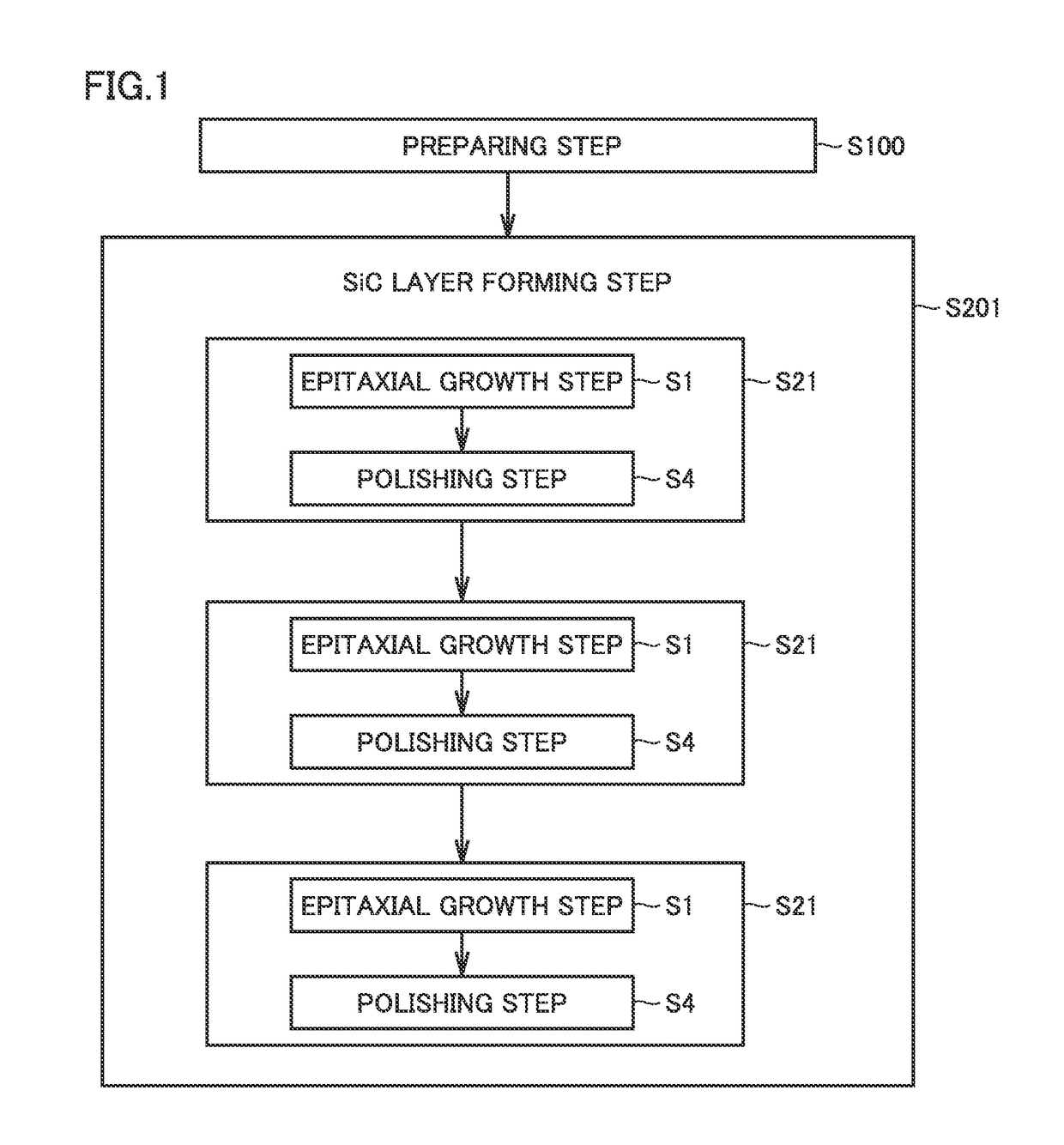
[0075]FIG. 1 is a flowchart schematically showing the first production method. With reference to FIG. 1, the first production method includes a preparing step (S100) and a first SiC layer forming step (S201). In the first production method, a series of steps (S21) including an epitaxial growth step (S1) and a polishing step (S4) are repeated twice or more in the first SiC layer forming step (S201). Here, FIG. 1 illustrates that the series of steps (S21) are repeated for 3 times, but the number of repetitions is not particularly limited as long as it is twice or more. However, in consideration of productivi...

second embodiment

Silicon Carbide Epitaxial Substrate

[0113]A second embodiment presents a SiC epitaxial substrate. FIG. 22 is a schematic view showing an example of a configuration of a SiC epitaxial substrate (wafer) according to the second embodiment. With reference to FIG. 22, SiC epitaxial substrate 100 includes SiC substrate 10 and third SiC layer 13 epitaxially grown on SiC substrate 10. SiC epitaxial substrate 100 preferably has a diameter of not less than 100 mm (for example, not less than 4 inches), and more preferably has a diameter of not less than 150 mm (for example, not less than 6 inches).

[0114]SiC epitaxial substrate 100 is typically obtained by the third production method mentioned above. Therefore, third SiC layer 13 has few defects resulting from inclusion of foreign matters and has high crystal quality. Moreover, because the surface of third SiC layer 13 is free of step-bunching, high reliability can be expected in an oxide film when the oxide film is formed thereon. Therefore, Si...

third embodiment

Silicon Carbide Semiconductor Device

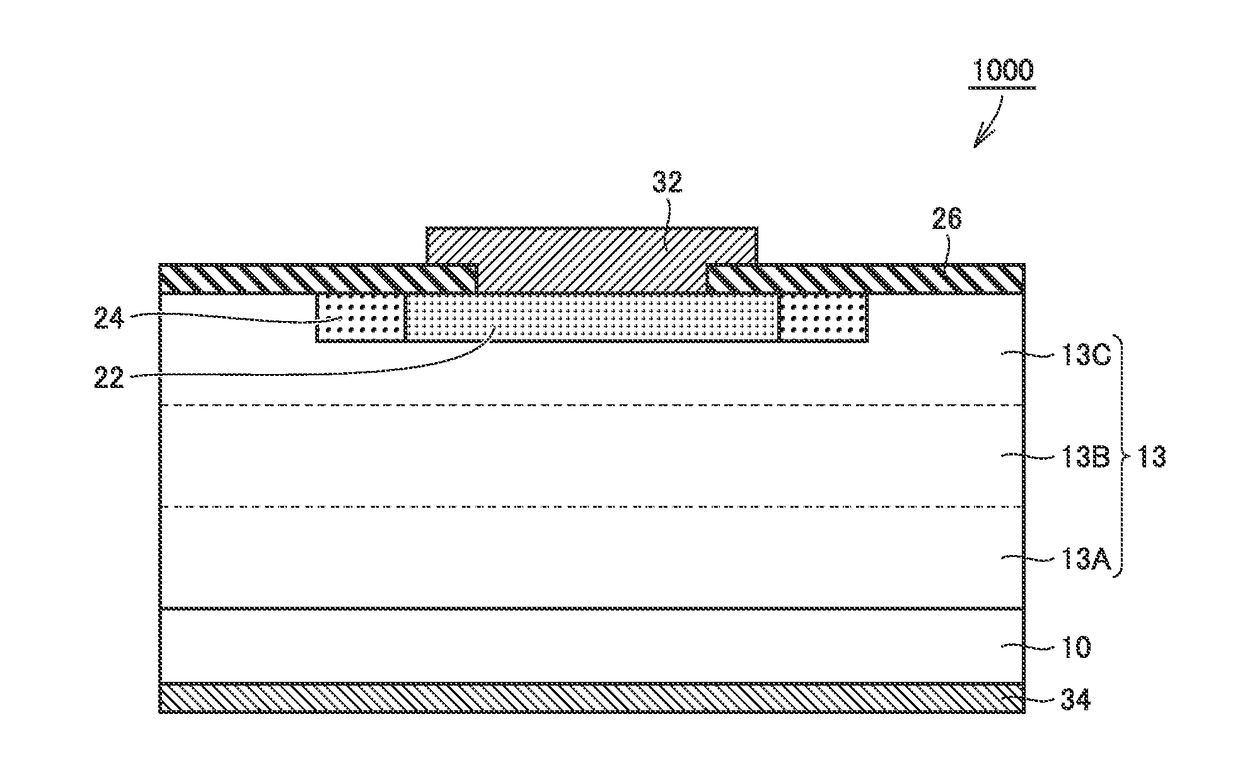
[0122]A third embodiment presents a SiC semiconductor device obtained using the SiC epitaxial substrate of the second embodiment. FIG. 25 is a schematic cross sectional view showing an example of a configuration of the SiC semiconductor device according to the third embodiment. A SiC semiconductor device 1000 shown in FIG. 25 is a planar type PiN diode. SiC semiconductor device 1000 includes SiC substrate 10 and third SiC layer 13 epitaxially grown thereon. Third SiC layer 13 includes first epitaxial layer 13A, second epitaxial layer 13B, and third epitaxial layer 13C, which have been grown stepwisely.

[0123]Third SiC layer 13 serves as a drift layer. In third SiC layer 13, a p+ region 22 and a JTE region 24 are formed by ion implantation, for example. JTE region 24 is a p type region, and serves to relax electric field concentration at an end portion of pn junction. Moreover, an oxide film 26 and an anode electrode 32 are provided on third SiC lay...


PUM

PropertyMeasurementUnit
thicknessaaaaaaaaaa
breakdown voltageaaaaaaaaaa
thicknessaaaaaaaaaa

Abstract

A method of producing a silicon carbide epitaxial substrate includes steps of: preparing a silicon carbide substrate; and forming a silicon carbide layer on the silicon carbide substrate. In this production method, in the step of forming the silicon carbide layer, a step of growing an epitaxial layer and a step of polishing a surface of the epitaxial layer are repeated twice or more.

Description

CROSS-REFERENCE TO RELATED APPLICATIONS[0001]This application is a Divisional of U.S. patent application Ser. No. 14 / 824,938, filed Aug. 12, 2015, which claims the benefit of Japanese Patent Application No. 2014-192522, filed Sep. 22, 2014.BACKGROUND OF THE INVENTION[0002]Field of the Invention[0003]The present invention relates to a method of producing a silicon carbide epitaxial substrate, a silicon carbide epitaxial substrate, and a silicon carbide semiconductor device.[0004]Description of the Background Art[0005]Silicon carbide (SiC), which has high dielectric breakdown electric field strength, is drawing attention as a material to replace silicon (Si) for a next-generation power semiconductor device (also referred to as “power device”). Particularly, since SiC is an indirect gap semiconductor and intrinsically has a long carrier lifetime, SiC is greatly expected for a high breakdown voltage bipolar semiconductor device in which an effect of conductivity modulation determines th...

Claims


Application Information

Patent Timeline
Patent Type & Authority Applications(United States)
IPC IPC(8): H01L29/16H01L21/02H01L29/861H01L21/324H01L21/04H01L29/36H01L21/306
CPCH01L29/1608H01L29/36H01L21/02378H01L21/02529H01L29/861H01L21/30625H01L21/324H01L21/0475H01L21/0262H01L21/02634H01L21/0445H01L21/02447H01L21/02587H01L21/02658H01L29/8611H01L29/32H01L29/6606H01L29/872H01L29/0615H01L29/7395H01L21/02664
Inventor HIYOSHI, TORU
Owner SUMITOMO ELECTRIC IND LTD
Why Eureka
Try Eureka