Device test method
a technology of device and electrode, applied in the direction of electrical programme control, program control, instruments, etc., can solve the problems of difficult arrangement of electrode pads, limited miniaturization, and increased number of electrodes of semiconductor devices
- Summary
- Abstract
- Description
- Claims
- Application Information
AI Technical Summary
Benefits of technology
Problems solved by technology
Method used
Image

Examples
Embodiment Construction
[0039]Hereinafter, embodiments of the present invention will be described with respect to the accompanying drawings.
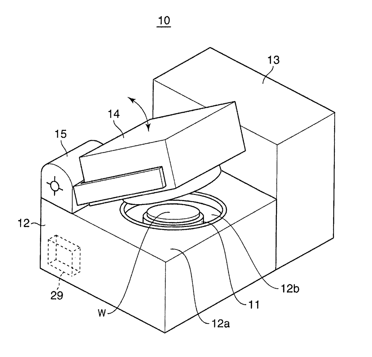
[0040]FIG. 1 is a perspective view schematically showing a configuration of a prober serving as a substrate test apparatus for performing a device test method in accordance with an embodiment.
[0041]In FIG. 1, a prober 10 (substrate test apparatus) includes a main body 12 which accommodates a stage 11 (mounting table) on which a wafer W is mounted, a loader 13 arranged adjacent to the main body 12, and a test head 14 arranged to cover the main body 12. The prober 10 measures electrical characteristics of a plurality of semiconductor devices formed on the wafer W having a large diameter of, e.g., 300 or 450 mm.
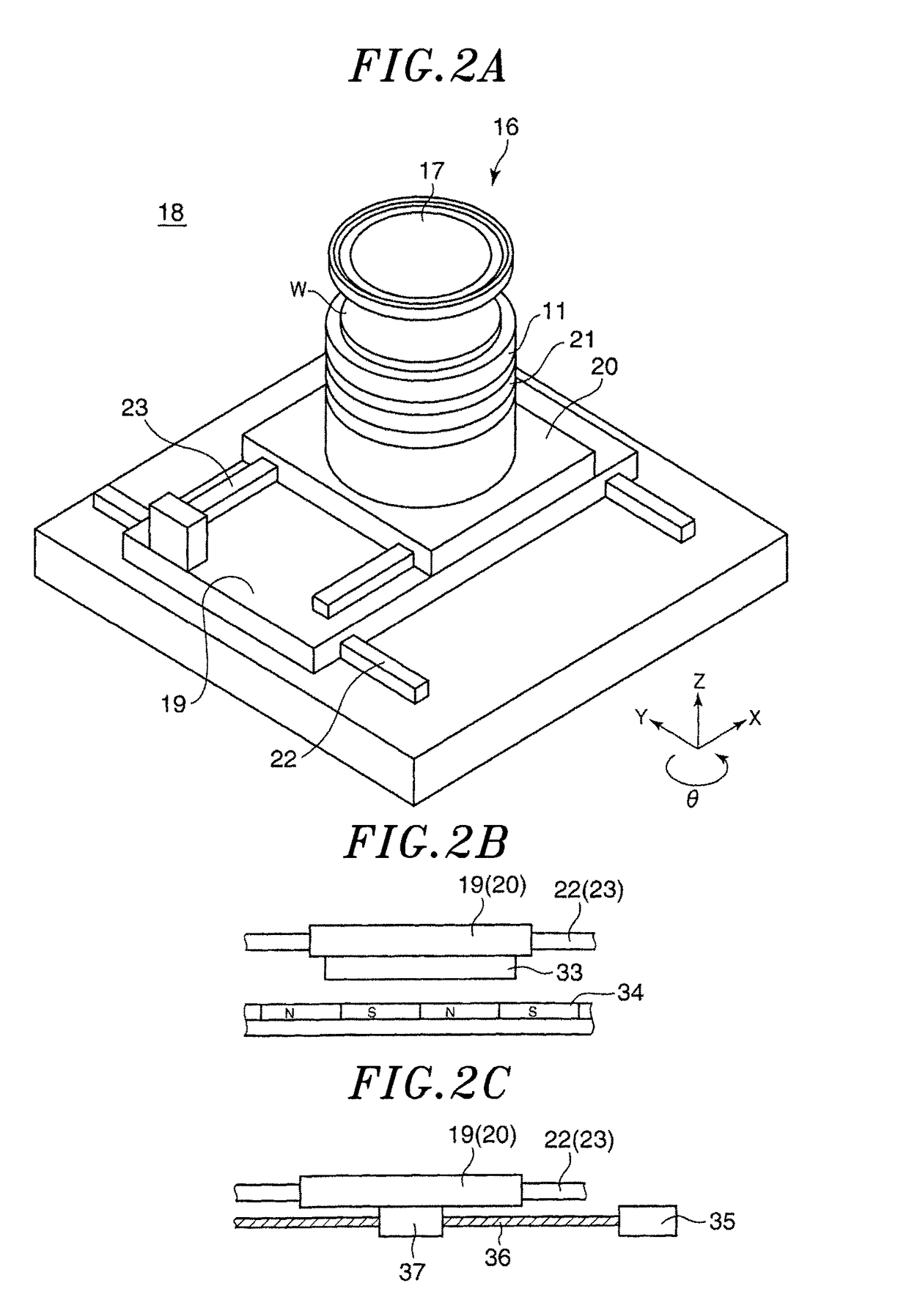
[0042]The main body 12 has a hollow case shape. At a ceiling portion 12a of the main body 12, an opening 12b is provided to be opened above the top of the wafer W mounted on the stage 11. A substantially disk-shaped probe card holder 16 is engaged with the opening ...
PUM
 Abstract
Description
Claims
Application Information