Method for automated assistance to design nonlinear analog circuit with transient solver

an analog circuit and solver technology, applied in the field of automatic assistance to design nonlinear analog circuits with transient solvers, can solve the problems of inability to reuse existing ip blocks, inability to solve problems such as inability to solve problems such as inability to solve problems such as inability to solve problems such as inability to solve problems such as inability to solve problems such as inability to solve problems such as inability to solve problems such as inability to solve problems such as inability to solve problems

Active Publication Date: 2018-02-20
CENT NAT DE LA RECHERCHE SCI +1
View PDF3 Cites 7 Cited by
  • Summary
  • Abstract
  • Description
  • Claims
  • Application Information

AI Technical Summary

Benefits of technology

[0059]With this method, the invention enables the circuit designer with more precise and / or relevant result in optimizing and designing of analog circuits, for example when it comes to large / quick signal circuits and / or with unstable or long duration variations.
[0061]The invention thus enables to improve the performance, precision and applicability of the current tools, and especially to enable a more efficient, precise and relevant analysis, simulation and optimization for nonlinear transient configurations, even for such heavily time dependent circuits, while keeping the significant and intuitive qualities of an analysis view such as described hereabove in relation with the CAIRO+ / CHAMS environment.
[0066]The computerized method of the invention may thus provide an automated assistance to design an analog non linear circuit relatively to its behavior under transient conditions, i.e. by taking into account its behavior in conditions where electrical parameter change quickly, and possibly in a non linear manner.

Problems solved by technology

However, analog / mixed-signal (AMS) traditionally tends to follow an ad hoc custom design process, with few or no possibilities of reusing existing IP blocks.
Also, when analog and digital blocks coexist on the same substrate, the analog portion can be more time-consuming to develop even though it may represent a smaller percentage of the chip area.
As a matter of fact, nonlinear unitary devices are very complex to model when used in an analog context, as their behavior is directly and immediately impacted by their unitary dimensions, such as the width (W) or length (L) of the physical transistors.
Until recently, capitalization of knowledge in analog circuits has been mainly limited to libraries of netlists, which describe structure rather than behavior.
However, such capitalization stands mainly on the human designer know-how and is deemed both a fastidious and very long work, while insufficiently efficient for automation.
The way previous or intermediate solutions are stored in this database does not guarantee, however, that this set of candidate solutions covers a relevant portion of the performance space.
The optimization algorithm itself is not able to construct knowledge of the search space based on its only experience.
However, as a difference with the digital context, design parameter ranges, especially for sizes, are very large and have a direct impact on analog behavior of every unitary device, even for a very small circuit.
As an example, a circuit of five transistors, if evaluated for 10 000 steps of one dimension, will give over 1020 possible dimensions to be simulated, many of which are technically not realistic nor interesting, which makes optimizing larger scale circuits very difficult if not impossible.
Optimizing thus need to make human heuristic hypothesis, that may easily lead to missing many interesting solutions.
Optimizing and designing of analog circuits may thus give a less precise or relevant result, for example when it comes to large / quick signal circuits and / or with unstable or long duration variations.
However, when the reactive effects of generally nonlinear components such as capacitors, inductors, diodes, MOS transistors, etc. are taken into account with simulation time, direct current solvers become insufficient, even in a multipoint sequence.

Method used


Image

  • Method for automated assistance to design nonlinear analog circuit with transient solver
  • Method for automated assistance to design nonlinear analog circuit with transient solver
  • Method for automated assistance to design nonlinear analog circuit with transient solver

Examples


case labeled bd

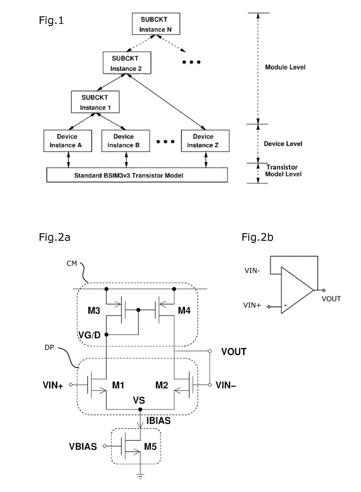
[0175]The content of various operators may depend on the type of connection existing between the currently processed transistor's terminals, which are illustrated in FIG. 11 and FIG. 12, where “D” is Drain terminal, “G” is Gain terminal, “S” is Source terminal, and “B” is Bulk terminal:[0176]case labeled NBND: The 4 terminals: D, G, S, B are independent, as illustrated in FIG. 11a for NMOS and in FIG. 12a for the PMOS;[0177]case labeled BND: The Source is connected to the Bulk, there are 3 independent terminals: D, G, S / B, as illustrated in FIG. 11b for NMOS and in FIG. 12b for the PMOS;[0178]case labeled NBD: The Drain is connected to the Gate, there are 3 independent terminals: D / G, S, B, as illustrated in FIG. 11c for NMOS and in FIG. 12c for the PMOS;[0179] The Drain is connected to the Gate and the Source is connected to the Bulk, there are 2 independent terminals: D / G, S / B, as illustrated in FIG. 11d for NMOS and in FIG. 12d for the PMOS.

[0180]FIG. 13, FIG. 14, FIG. 15 and FIG...

case bd

[0188]These four operator terminal currents are computed from the 3 MOS currents “iD” (flowing into the Drain), “iG” (into the Gate) and “iB” (flowing out of the Bulk), in a different way for each of the four configurations NBND, NBD, BND, BD, as follows:[0189]for an NMOS transistor:[0190]case NBND:[0191]iD_op=iD[0192]iB_op=−iB[0193]iG_op=iG[0194]iS_op=−iD−iG+iB[0195]case NBD:[0196]iD_op=iD+iG[0197]iB_op−iB[0198]iG_op=iG[0199]iS_op=−iD−iG+iB[0200]case BND:[0201]iD_op=iD[0202]iB_op=−iB[0203]iG_op=iG[0204]iS_op=−iD−iG[0205][0206]iD_op=iD+iG[0207]iB_op=−iB[0208]iG_op=iG[0209]iS_op=−iD−iG[0210]for an PMOS transistor:[0211]case NBND:[0212]iD_op=iD[0213]iB_op=−iB[0214]iG_op=iG[0215]iS_op=−iD−iG+iB[0216]case NBD:[0217]iD_op=iD+iG[0218]iB_op=−iB[0219]iG_op=iG[0220]iS_op=−iD−iG+iB[0221]case BND:[0222]iD_op=ID[0223]iB_op=−iB[0224]iG_op=iG[0225]iS_op=−iD−iG[0226]case BD:[0227]iD_op=iD+iG[0228]iB_op=−iB[0229]iG_op=iG[0230]iS_op=−iD−iG

[0231]This computing is done here by a “Compute Operator Curr...


PUM


Abstract

A method is provided for providing an automated assistance to design an analog non linear circuit under transient conditions, and to a corresponding system. The method enables the circuit designer to consider with simulation the time reactive effects of generally nonlinear components, while keeping the significant and intuitive qualities of an analysis view design tool like the CAIRO+ / CHAMS environment. The method includes at least a transient instant solving procedure producing a numerical simulation that uses a given set of sizes and biases to provide a set of local behavior parameters in at least one node at current time. This transient instant solving procedure includes an incremental iteration under transient conditions of an evaluation in an analysis view of a dependency graph of the functional structure of the circuit. An optional transient analysis performs a numerical simulation to provide a time dependent behavior simulation of the circuit, and a performance evaluation.

Description

INTRODUCTION[0001]The present invention relates to a method for providing an automated assistance to design and / or simulate an analog non linear circuit under transient conditions, and to a system implementing such a method.[0002]With this method, the invention enables the circuit designer with more precise and / or relevant result in optimizing and designing analog circuits, for example when it comes to large / quick signal circuits and / or with unstable or long duration variations. It becomes possible to take into account with simulation the time reactive effects of generally nonlinear components, such as capacitors, inductors, diodes, MOS transistors, or other heavily time dependent circuits, while keeping the significant and intuitive qualities of an analysis view already implemented in CAIRO+ / CHAMS environment, though currently only for Direct Current solving.[0003]Said method comprises at least a transient instant solving procedure producing a numerical simulation that uses a given...

Claims


Application Information

Patent Timeline
Patent Type & Authority Patents(United States)
IPC IPC(8): G06F17/50
CPCG06F17/5063G06F17/5036G06F30/36G06F30/367
Inventor ISKANDER, RAMYLOUERAT, MARIE-MINERVEKAISER, ANDREASJAVID, FARAKH
Owner CENT NAT DE LA RECHERCHE SCI
Why Eureka
Try Eureka