Light emitting diode structure, light emitting diode device and the manufacturing method thereof

a technology of light emitting diodes and manufacturing methods, applied in the direction of basic electric elements, semiconductor devices, electrical devices, etc., can solve the problems of unmatched heat expansion coefficient of underfill materials, and increased risk in the following manufacturing process, so as to enhance the light emitting performance of the light emitting diodes and reduce warpage

Active Publication Date: 2018-05-08
LITE ON OPTO TECH (CHANGZHOU) CO LTD +1
View PDF10 Cites 0 Cited by
  • Summary
  • Abstract
  • Description
  • Claims
  • Application Information

AI Technical Summary

Benefits of technology

[0005]In addition, the instant disclosure further provides a light emitting diode structure and a light emitting diode device comprising the light emitting diode structure for solving the deformation and cave-in problem generated after the laser lift-off process to reduce the warpage and enhance the light emitting performance of the light emitting diode device.

Problems solved by technology

However, the heat expansion coefficient of the underfill material and the chip is not matched and the risk in the following manufacturing process is increased.

Method used


Image

  • Light emitting diode structure, light emitting diode device and the manufacturing method thereof
  • Light emitting diode structure, light emitting diode device and the manufacturing method thereof
  • Light emitting diode structure, light emitting diode device and the manufacturing method thereof

Examples


Embodiment Construction

[0022]Reference will now be made in detail to the exemplary embodiments of the instant disclosure, examples of which are illustrated in the accompanying drawings. Wherever possible, the same reference numbers are used in the drawings and the description to refer to the same or like parts.

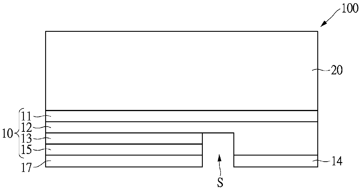
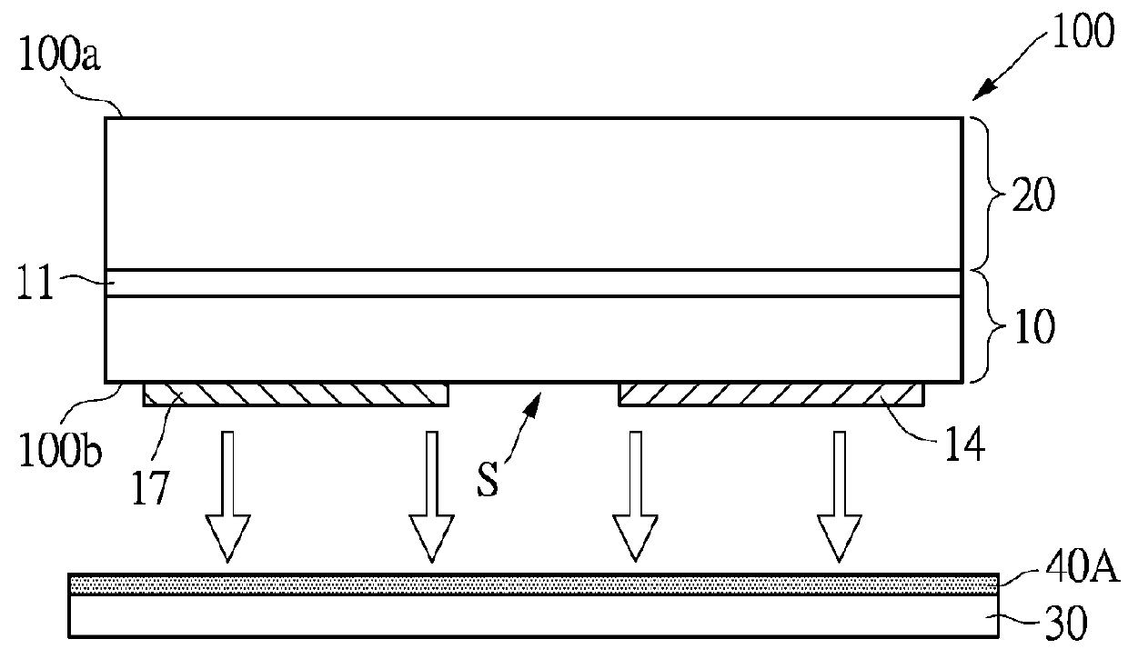
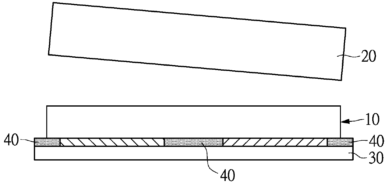
[0023]Please refer to FIG. 1. FIG. 1 is a schematic view of the fixing of the chip of the light emitting diode structure of the instant disclosure. The instant disclosure provides a method for manufacturing a light emitting diode structure. First, providing a flip-type chip 100, the flip-type chip has a growth substrate 20, an epitaxial structure 10 formed on the growth substrate 20 and at least a pair of chip metal pads 14, 17. A gap S is located between the pair of chip metal pads 14, 17.

[0024]In the present embodiment, the growth substrate can be a sapphire substrate, and each flip-type chip has a first surface 100a (the upper side shown in FIG. 1) and a second surface 100b (the lower side shown ...


PUM


Abstract

A method for manufacturing a light emitting diode structure uses a removable prefilled layer to attach the flip-type chip on a temporary substrate. A growth substrate of the flip-type chip is removed by laser lift-off, and then the light emitting diode structure is attached to a transparent support body. Lastly, the temporary substrate and the prefilled layer are removed.

Description

BACKGROUND1. Technical Field[0001]The instant disclosure relates to a method for manufacturing a light emitting diode (LED) structure, in particular, to a method related to an LED chip without a growth substrate employing laser lift-off to be removed from the LED chip and the process for forming the same. In addition, the LED structure and device manufactured by the above method are also included.2. Description of Related Art[0002]Generally, in order to solve the deformation and cave-in problem which are happened in producing thin film LED chips during sapphire substrate removed by laser lift-off, an underfill material (or referred to as a buffering material) is introduced for supporting the epitaxy layer. However, the heat expansion coefficient of the underfill material and the chip is not matched and the risk in the following manufacturing process is increased.SUMMARY[0003]The instant disclosure provides a method for manufacturing an LED structure to solve the deformation and cave...

Claims


Application Information

Patent Timeline
Patent Type & Authority Patents(United States)
IPC IPC(8): H01L33/22H01L33/24H01L33/00H01L33/10H01L33/50
CPCH01L33/0079H01L33/10H01L33/502H01L33/24H01L2933/0058H01L2933/0033H01L33/60H01L33/0093H01L33/54
Inventor CHIEN, I-CHENHSU, SHIH-CHANG
Owner LITE ON OPTO TECH (CHANGZHOU) CO LTD
Why Eureka
Try Eureka