
Plasma display device and image processing method thereof

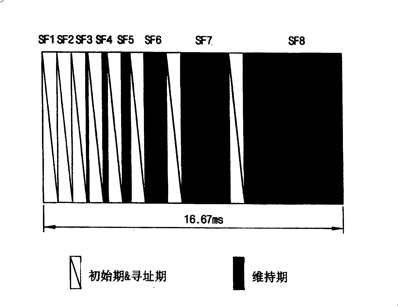
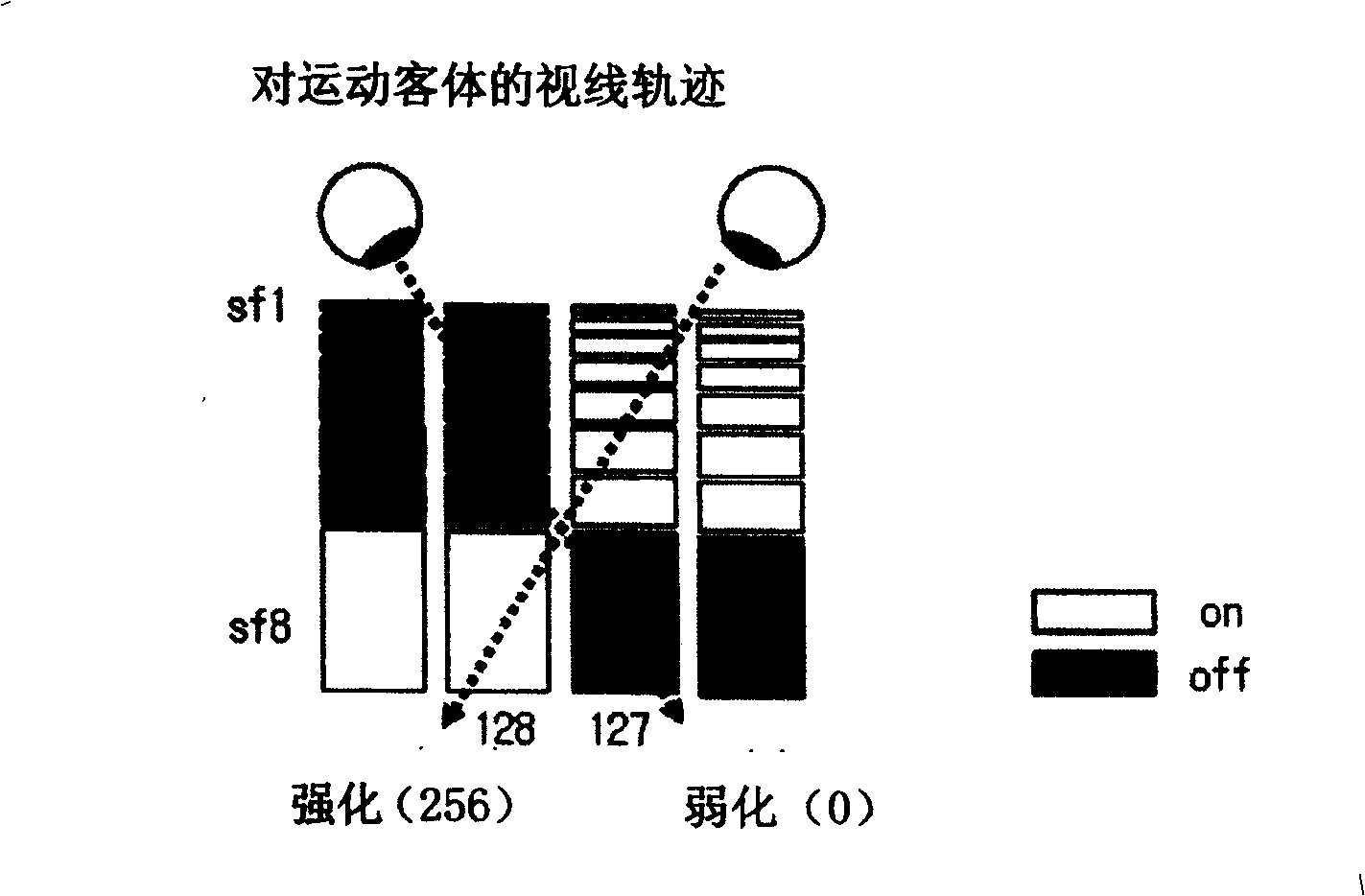
A display device and image processing technology, applied in identification devices, static indicators, instruments, etc., can solve the problems of rising unit price of plasma display device production and complex algorithm composition, and achieve the effect of suppressing animation false contour and reducing unit price of production

Inactive Publication Date: 2008-09-03
LG ELECTRONICS(NANJING) PLASMA CO LTD
View PDF3 Cites 0 Cited by
  • Summary
  • Abstract
  • Description
  • Claims
  • Application Information

AI Technical Summary

Problems solved by technology

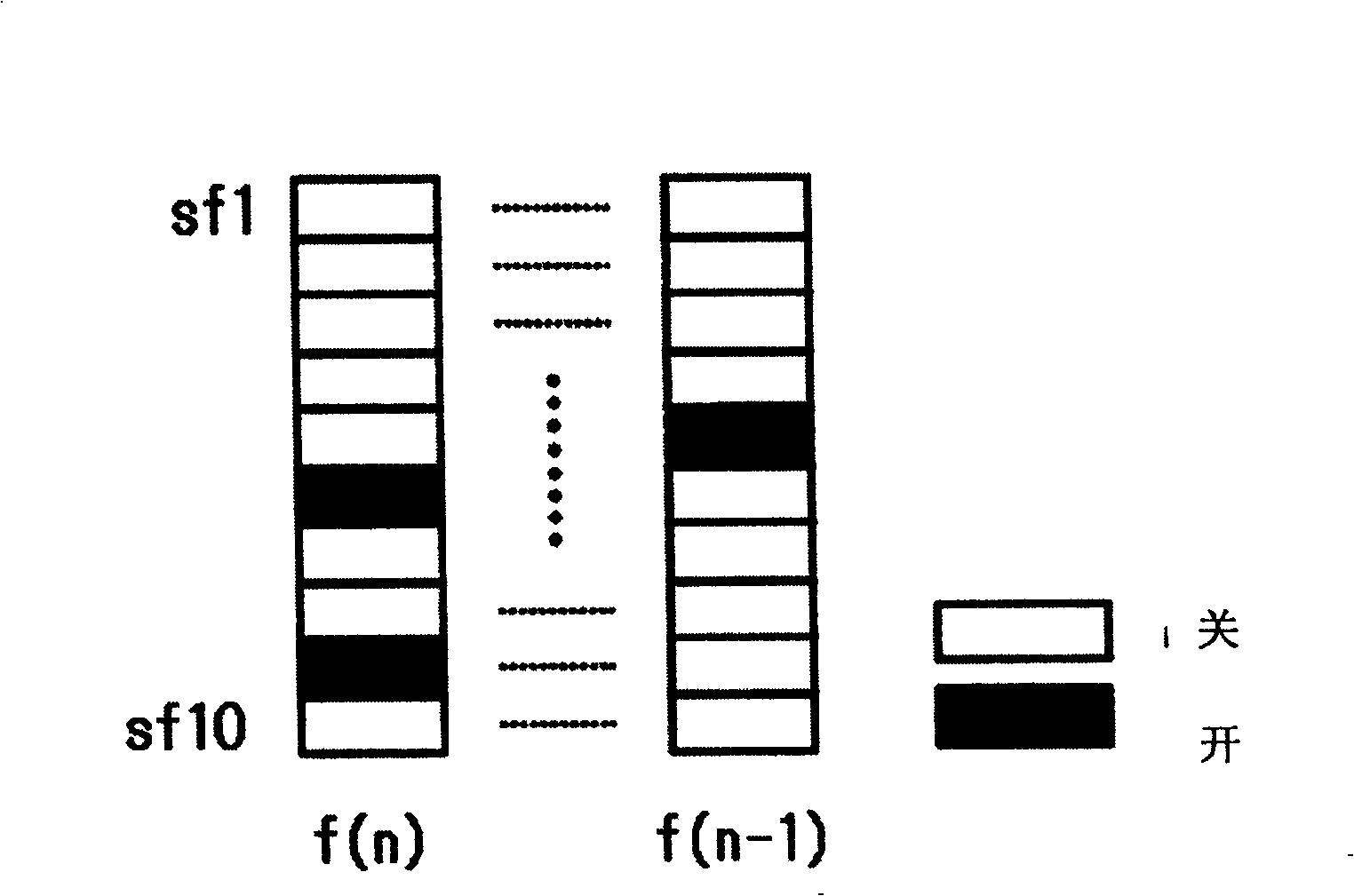
[0017] Here, the prior art has the following problem: in order to detect MPD, the subfield mapping code of the previous picture frame and the subfield mapping code of the current picture frame are used, therefore, the subfield mapping code of the subfield mapping code of the previous picture frame needs to be stored memory
Such a subfield mapping code memory increases the production unit price of the plasma display device, and since the subfield mapping code of the previous picture frame is compared with the subfield mapping code of the current picture frame, the algorithm configuration is complicated.

Method used


Image

  • Plasma display device and image processing method thereof
  • Plasma display device and image processing method thereof
  • Plasma display device and image processing method thereof

Examples


Embodiment Construction

[0053] Next, specific embodiments according to the present invention will be described with reference to the accompanying drawings.

[0054] FIG. 4 is a schematic diagram illustrating a plasma display device according to an embodiment of the present invention.

[0055] As shown in FIG. 4 , a plasma display device according to an embodiment of the present invention includes: a picture frame memory 400, a moving area detector 410, a reverse gray scale corrector 420, a half-tone device 430, an MPD detector 440, a false contour Compensation area determiner 450 , false contour compensator 460 .

[0056] The picture frame memory 400 stores video signals input from the outside in units of picture frames for the moving area detector 410 to compare the video signals of the previous picture frame (n-1) and the current picture frame (n) to detect a moving area. That is, the video signal of the previous picture frame (n-1) previously stored in the picture frame memory 400 is compared wit...


PUM


Abstract

A plasma display device and an image processing method thereof are provided to effectively detect an MPD(Moving Picture Distortion) by using an image signal which input from the outside. A moving region detecting unit(410) compares an image signal of the previous frame with an image signal of the present frame in their gradation values and detects the moving region of the image. An MPD detecting unit(440) calculates an MPD value between adjacent pixels by using a subfield mapping code of the image signal in the previous frame and detects an MPD region. A pseudo contour compensating region determining unit(450) determines a pseudo contour of an image in a screen of the present frame by using the moving region detecting information and the MPD detecting information. A pseudo contour compensating unit(460) performs mapping of the image signal in the pseudo contour compensating region into a pseudo contour compensating subfield.

Description

1. Technical field [0001] The present invention relates to a plasma display device, more specifically a plasma display device capable of detecting MPD (Moving Picture Distortion) more effectively and an image processing method thereof. 2. Background technology [0002] Generally, a plasma display apparatus (Plasma Display Apparatus) includes a plasma display panel in which a partition wall formed between a front panel and a rear panel forms a unit cell. Each cell is filled with charging and discharging gas such as neon (Ne), helium (He) or a mixed gas of neon and helium (Ne+He), and an inert gas containing a small amount of xenon. When discharging by high-frequency voltage, the inert gas emits vacuum ultraviolet rays (Vacuum Ultraviolet rays), so that the phosphors formed between the partition walls emit light to display the screen. Such a plasma display device has a thin and light structure, and is attracting attention as a next-generation display device. [0003] figure...

Claims


Application Information

Patent Timeline
Patent Type & Authority Patents(China)
IPC IPC(8): G09G3/28G09G3/20H01J17/49G09F9/313G09G3/296G09G3/291
CPCG09G3/2007G09G3/28G09G3/291G09G3/296
Inventor 白承杰
Owner LG ELECTRONICS(NANJING) PLASMA CO LTD
Learn More