High-efficiency neutron detectors and methods of making same

a neutron detector and high-efficiency technology, applied in the field of neutron detectors and methods of making same, can solve the problems of reducing the energy transfer to the semiconductor detector, gd-based films are less attractive for devices, and thermal neutron detection efficiency is limited to only 4%, so as to achieve compact and rugged, detect the effect of efficiency and thinness

Active Publication Date: 2005-11-24
RGT UNIV OF MICHIGAN
View PDF7 Cites 111 Cited by
  • Summary
  • Abstract
  • Description
  • Claims
  • Application Information

AI Technical Summary

Benefits of technology

[0043] An object of the present invention is to provide neutron detectors that have detection efficiencies many times greater than present neutron detectors while remaining relatively thin, compact and rugged. The detectors detect neutrons of any energy including thermal neutrons.

Problems solved by technology

As a result, Gd-based films are less attractive for devices where background gamma ray contamination is a problem.
Thus far, thermal neutron-detection efficiencies have been limited to only 4% for 6LiF and 10B single-coated devices.
Reaction product self-absorption reduces the energy transferred to the semiconductor detector, and ultimately limits the maximum film thickness that can be deposited over the semiconductor device.
If the neutron reaction film thickness is thin, coincident charged particle emissions from a single neutron absorption event can be measured simultaneously by both detectors if operated individually, thus giving rise to the erroneous recording of two neutron interaction events when only one actually occurred.
Neutron-detection efficiency is limited for single coated devices since charged particle reaction products have limited ranges in the neutron reactive thin film.

Method used


Image

  • High-efficiency neutron detectors and methods of making same
  • High-efficiency neutron detectors and methods of making same
  • High-efficiency neutron detectors and methods of making same

Examples


Embodiment Construction

Multi-Layered Films for Improved Efficiency

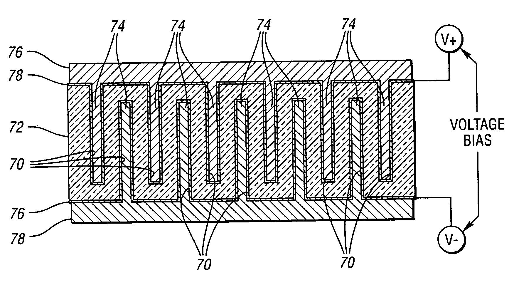
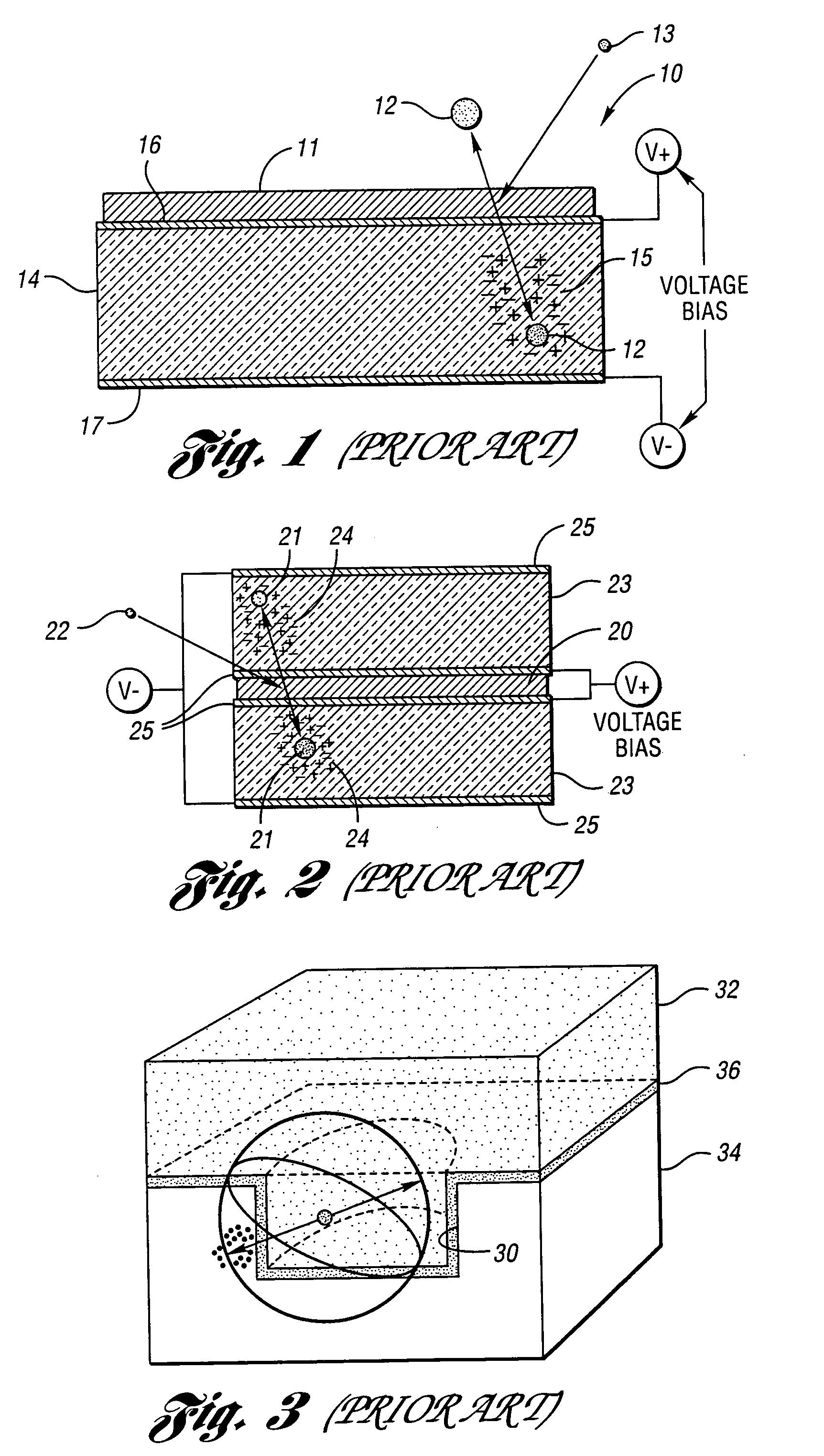
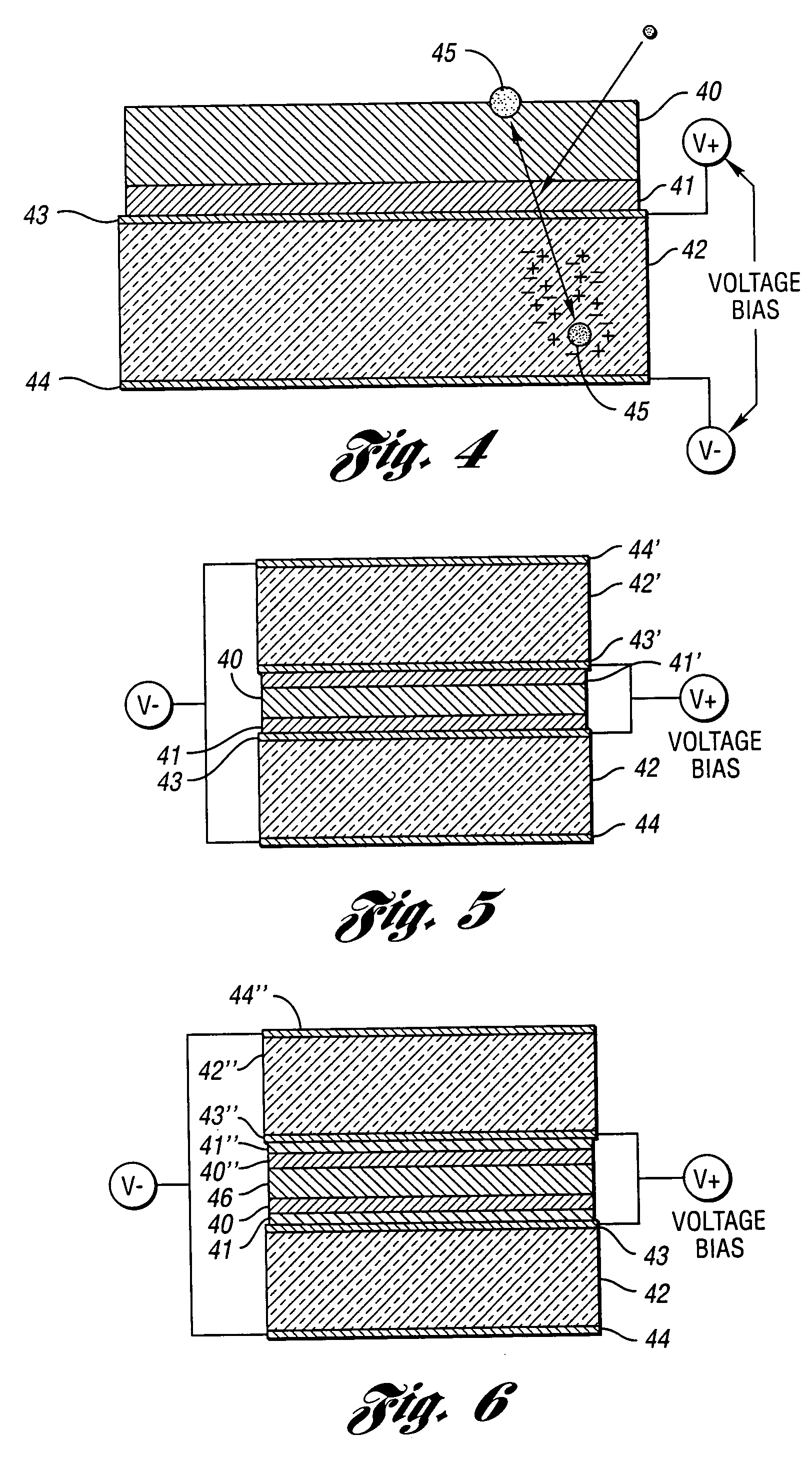
[0115] Referring now to FIG. 4, an embodiment of the invention is shown in which the simplistic prior art approach for the coating of a detector has been modified to incorporate multiple films 40 and 41. The neutron reactive films 40 and 41 may include, but are not limited to, various compounds and concentrations of boron, lithium, lithium fluoride, gadolinium and cadmium. Fissionable materials such as, but not limited to U235, Pu, Th are also applicable. The device can have two or more different neutron reactive films 40 and 41 placed upon the detector surface. The semiconductor material 42 may be composed of a variety of materials, including, but not limited to, silicon, silicon carbide, gallium arsenide, gallium nitride, indium phosphide, cadmium telluride, cadmium-zinc-telluride, gallium phosphide, mercuric iodide, lead iodide, and variations of these aforementioned semiconductors. The detector has conductive contacts 43 and 44, one c...


PUM


Abstract

Neutron detectors, advanced detector process techniques and advanced compound film designs have greatly increased neutron-detection efficiency. One embodiment of the detectors utilizes a semiconductor wafer with a matrix of spaced cavities filled with one or more types of neutron reactive material such as 10B or 6LiF. The cavities are etched into both the front and back surfaces of the device such that the cavities from one side surround the cavities from the other side. The cavities may be etched via holes or etched slots or trenches. In another embodiment, the cavities are different-sized and the smaller cavities extend into the wafer from the lower surfaces of the larger cavities. In a third embodiment, multiple layers of different neutron-responsive material are formed on one or more sides of the wafer. The new devices operate at room temperature, are compact, rugged, and reliable in design.

Description

CROSS-REFERENCE TO RELATED APPLICATION [0001] This application claims the benefit of U.S. provisional application Ser. No. 60 / 422,148, filed Oct. 29, 2002 and entitled “High Efficiency Neutron Detectors.”STATEMENT REGARDING FEDERALLY SPONSORED RESEARCH OR DEVELOPMENT [0002] This invention was made with Government support under Contract No. W-31-109-ENG-38 from the U.S. Department of Energy (DOE). The Government has certain rights in this invention.BACKGROUND OF THE INVENTION [0003] 1. Field of the Invention [0004] This invention relates to neutron detectors, methods of making same, and in particular, to high-efficiency neutron detectors and methods of making same. [0005] 2. Background Art [0006] Semiconductor detectors coated with neutron reactive materials offer an alternative approach to scintillator-based neutron imaging devices for neutron radiography (normally scintillating screens coupled to photographic film or to other photorecording devices). The detectors also offer an alt...

Claims


Application Information

Patent Timeline
Patent Type & Authority Applications(United States)
IPC IPC(8): G01T1/185G01T3/00G01T3/08
CPCG01T1/185G01T3/08G01T3/00
Inventor MCGREGOR, DOUGLAS S.KLANN, RAYMOND
Owner RGT UNIV OF MICHIGAN
Why Eureka
Try Eureka