

Apparatus and method for processing substrate
A processing device and processing method technology, applied in chemical instruments and methods, cleaning methods using liquids, spraying devices, etc., can solve the problems of difference, poor reactivity, and inability to uniformly process substrates, etc.
- Summary
- Abstract
- Description
- Claims
- Application Information
AI Technical Summary
Problems solved by technology
Method used
Image

Examples
Embodiment Construction
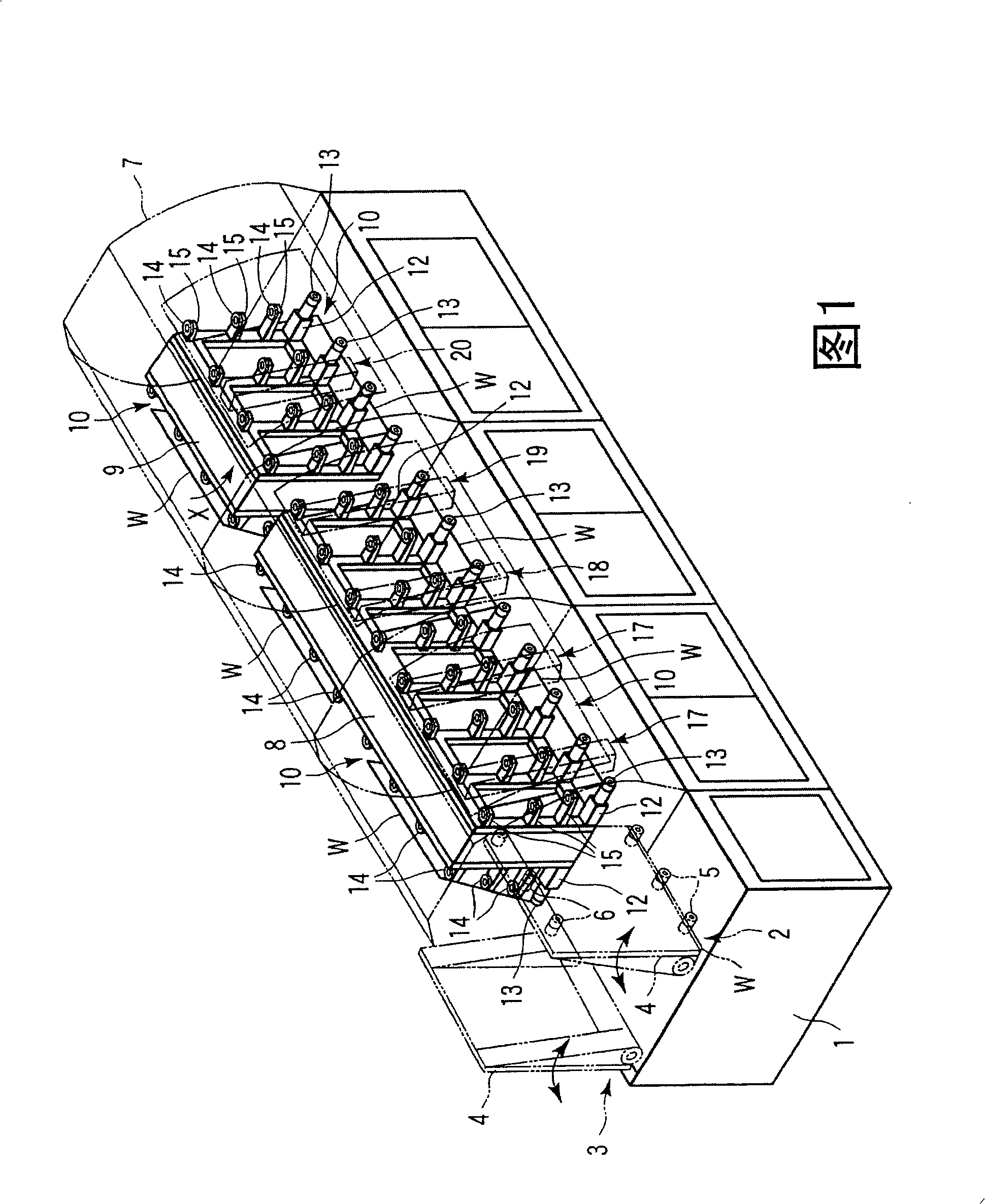
[0052] Hereinafter, one embodiment of the present invention will be described with reference to the drawings.
[0053] 1 to 8 show a first embodiment of the present invention. The treatment device shown in FIG. 1 has a base station 1 . At one longitudinal end of the upper surface of the base 1, a loading section 2 and an unloading section 3 are arranged laterally apart. The loading part 2 and the unloading part 3 have a rectangular plate-shaped supporting member 4, which can be driven to swing along the lateral direction of the base 1 indicated by the arrow, using the lower end as a fulcrum.
[0054] At the lower end of one side of the loading part 2 and the unloading part 3 (only the loading part 2 is shown in the figure), a plurality of lower supporting rollers 5 are arranged at regular intervals, and a plurality of upper supporting rollers are arranged at prescribed intervals at the upper end. 6. The lower backup roller 5 is rotationally driven by a driving source not sh...
PUM
 Abstract
Description
Claims
Application Information