Carrying structure for electron element

A technology of electronic components and bearing structures, applied in the field of bearing structures of electronic components, can solve the problems that do not conform to the development trend of light, thin and short semiconductor packages, reduce the flexibility of circuit layout on the surface of circuit boards, and limit the number of passive components. Achieve the effect of reducing reliability risk, improving quality and reliability, and good electrical function

Active Publication Date: 2008-12-03
PHOENIX PRECISION TECH CORP
View PDF3 Cites 0 Cited by
  • Summary
  • Abstract
  • Description
  • Claims
  • Application Information

AI Technical Summary

Problems solved by technology

Restricting the installation position of passive components will reduce the flexibility of circuit board surface circuit layout (Routability); at the same time, the position of soldering pads needs to be considered, resulting in the limitation of the number of passive components; even the number of passive components layout increases with the semiconductor The requirements for high performance of the package are relatively increased. If the existing method is adopted, the surface of the circuit board must accommodate multiple semiconductor chips and a large number of passive components at the same time, forcing the package to further increase the volume, which does not meet the requirements of light, thin and short semiconductor packages. development trend

Method used


Image

  • Carrying structure for electron element
  • Carrying structure for electron element
  • Carrying structure for electron element

Examples


Embodiment 1

[0024] The load-bearing structure of the electronic component in this embodiment 1 includes: at least one support plate, the support plate is provided with at least one opening; at least one electronic component has an active surface and a non-active surface, and is arranged in the corresponding opening of the support plate; And at least one adhesive layer formed on the surface of the support plate, wherein the adhesive layer partially fills the gap between the opening and the electronic component, so that the electronic component is fixed in the opening of the support plate.

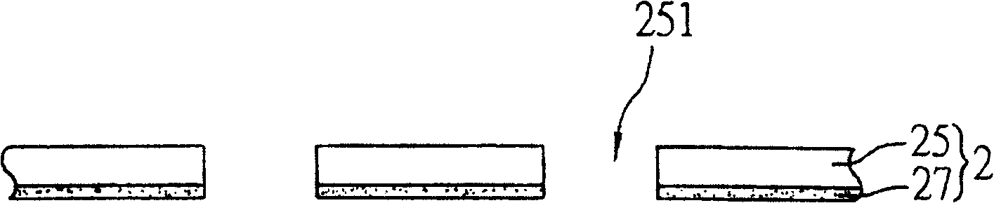
[0025] Figure 2A and Figure 2BIt is a schematic diagram of the carrying structure of the electronic component of the present invention. As shown in the figure, the supporting structure 2 is provided with a support plate 25 , and the support plate 25 is provided with at least one opening 251 , wherein an adhesive layer 27 is formed on the surface of the support plate 25 . In the present embodiment 1,...

Embodiment 2

[0030] The carrying structure of the electronic component in the second embodiment includes: at least one first support plate and a second support plate, the first support plate and the second support plate are provided with at least one opening; at least one adhesive layer is formed on the first Between the support plate and the second support plate, and at least one electronic component has an active surface and a non-active surface, which are arranged in corresponding openings of the first support plate and the second support plate. Wherein the adhesive layer partially fills the gap between the openings of the first support plate and the second support plate and the electronic component, so that the electronic component is fixed in the openings of the first support plate and the second support plate.

[0031] Figure 3A It is a schematic diagram of Embodiment 2 of the carrying structure of the electronic component of the present invention. The biggest difference between Em...

Embodiment 3

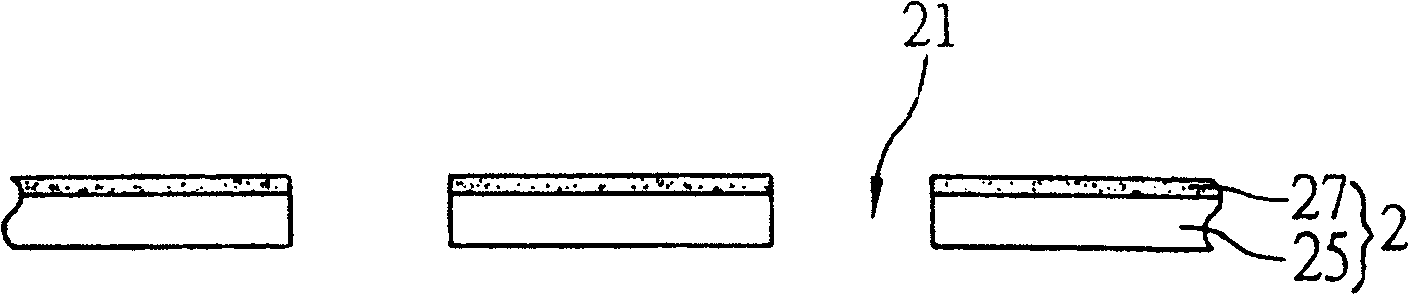
[0037] Figure 4A to Figure 4C It is a schematic diagram of Embodiment 3 of the carrying structure of the electronic component of the present invention, wherein the same or similar components as those of the above embodiment are represented by the same or similar component symbols.

[0038] Such as Figure 4A As shown, the electronic component carrying structure includes: a support plate 25, at least one electronic component 23 and an adhesive layer 27 formed on the surface of the support plate.

[0039] The support plate 25 is provided with at least one opening 251 , wherein, although the supporting structure 2 is shown as a two-layer structure including the support plate 25 and the adhesive layer 27 in the drawing, it is not limited thereto.

[0040] The electronic component 23 has an active surface and a non-active surface. In the third embodiment, the active surface of the electronic component 23 is located on the upper surface, and the non-active surface of the electroni...


PUM


Abstract

This invention provides one electron element supportive structure, which comprises the following parts: at least one supportive board with at least one opening; at least one electron element with main interface and non active surface set in the opening of supportive board and at least one adhesive layer for form supportive board surface, wherein, the adhesive layer part is filled into gap between opening and electron element to fix the electron element into the opening holes.

Description

technical field [0001] The invention relates to a bearing structure for electronic components, in particular to a bearing structure for bearing and fixing electronic components. Background technique [0002] Since the introduction of flip chip packaging (Flip Chip package) technology by IBM in the early 1960s, compared with wire bonding (Wire bonding) technology, flip chip technology is characterized by the electrical connection between the semiconductor chip and the circuit board. Solder bumps instead of normal gold wires. The advantage of flip-chip technology is that it can increase the packaging density and reduce the package size. At the same time, the flip-chip technology does not need to use metal wires, so it can improve electrical performance and meet the needs of high-density and high-speed semiconductor devices. [0003] In the existing flip-chip technology, the active surface of the semiconductor integrated circuit (IC) chip is equipped with electrode pads (Elect...

Claims


Application Information

Patent Timeline
Patent Type & Authority Patents(China)
IPC IPC(8): H01L25/00H01L23/498H01L23/50
CPCH01L24/96H01L2224/12105H01L2224/19H01L2924/14H01L2924/18162H01L2924/00H01L2924/00012
Inventor 许诗滨
Owner PHOENIX PRECISION TECH CORP
Why Eureka
Try Eureka